Тепло, которое стало светом: кремниевый путь к энергии экспресс
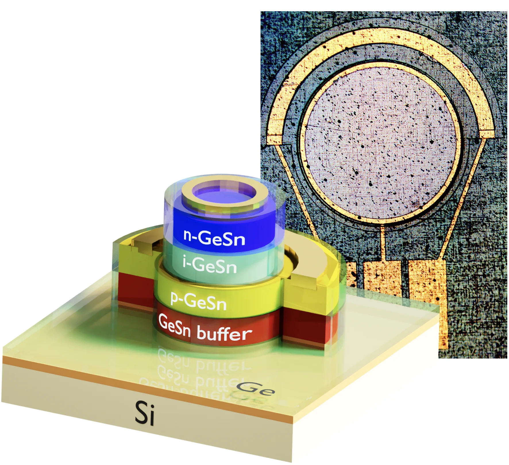
Раскалённая печь в цеху или горячий выхлоп турбины — это не просто жар, а свет, который человеческий глаз не видит. Обычные солнечные батареи ловят видимый свет, а здесь нужен приёмник для невидимого теплового излучения. Группа исследователей впервые собрала такой приёмник из сплава германия с оловом — материала, который можно выращивать прямо на кремниевых пластинах, как обычные компьютерные чипы.
Испытали образец размером с булавочную головку: направили на него луч лазера с длиной волны 2,33 микрона и свет от нагретой до 1500 кельвинов керамической пластины. Прибор выдал ток, хотя и скромный — мощность составила около 0,41 милливатта с квадратного сантиметра. Это в сотни раз меньше, чем у дорогих аналогов из арсенида индия, но важно другое: материал работает.
Расчёты показали, что главная беда — дефекты в кристалле, из-за которых носители заряда гибнут по пути. Если их убрать, мощность вырастет до 1 ватта с квадратного сантиметра — в тысячи раз. Тогда такой элемент сможет питать датчики на заводах, в космосе или даже в быту, собирая тепло, которое сегодня просто улетает в трубу.
Оригинальная аннотация
как её написали авторы, на английском arXiv:2602.21392
Thermophotovoltaic (TPV) cells are increasingly attractive for applications in industrial waste heat harvesting, aerospace energy management, and compact power generation. Deploying midwave-infrared (MWIR) TPV in practical applications requires narrow-bandgap semiconductors that not only absorb low-energy photons but also integrate with scalable, low-cost platforms. Although high-performance TPV devices have been demonstrated using III-V materials such as InAs, GaSb, and InGaAs(P), their use remains limited by cost and substrate size. With this perspective, narrow bandgap GeSn alloys are a promising alternative that extend group-IV absorption into the MWIR while being silicon-compatible. Although the potential of GeSn TPV cells has been predicted, no experimental demonstration has been reported. Here, proof-of-concept Ge$$_{0.91}$$Sn$$_{0.09}$$ p-i-n TPV diodes (1 mm diameter) grown on silicon were fabricated and their performance was benchmarked against commercial InAs and extended-InGaAs devices. Measurements at 300 K under 2.33 $$\mu$$m laser and $$\sim$$1500 K SiC Globar illumination revealed peak responsivity of $$\sim$$ 0.2 A/W at $$\sim$$ 1.7 $$\mu$$m, and an output power of $$\sim$$ 0.41 mW/cm$$^2$$. These devices show trends comparable to those of the InAs diode under identical conditions, although at reduced absolute levels. To assess the intrinsic performance potential, Poisson-drift-diffusion modeling incorporating experimentally calibrated emitter emissivity predicts power densities exceeding 1 W/cm$$^2$$ under moderate MWIR thermal illumination, indicating that the present devices operate far below their fundamental limits and are primarily constrained by defect-assisted recombination and transport losses. These results establish GeSn as a scalable, silicon-compatible MWIR TPV platform and highlight a larger performance potential achievable through material and device optimization.
Сплав германия с оловом можно нанести на кремний так же, как глазурь на печенье, — тонким слоем, и он не потрескается.