How a Polymer Film Tames a Molybdenum Disulfide Transistor express
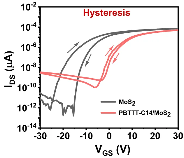
A transistor is like a faucet that controls the flow of electrons. In the normal state, the faucet should be closed, opening only on command. But transistors made of molybdenum disulfide, thin layers of this material are a promising replacement for silicon, behave like a leaky faucet: they conduct current even without a control signal. This is called depletion mode. They also have poor memory: after a "close" command, the faucet doesn't close immediately, and sometimes it gets stuck altogether. This is called hysteresis.
Researchers found a way to fix both defects at once. They applied a thin layer of the polymer PBTTT-C14 to the transistor's surface — an organic material that can transport positive charges. The layer acts as a gasket that redistributes charges at the interface between the two materials. As a result, the faucet starts working correctly: the voltage at which the transistor turns on shifted from -9.6 volts to +5.9 volts. This means that without a command, it is now closed, not open. Hysteresis decreased from 8.8 volts to 1.3 volts — memory became much better.
To make sure it was indeed the charge transfer that mattered, the researchers tested another polymer, P3HT, which has similar energy levels. It produced the same effect: the transistor switched to enhancement mode, and hysteresis was suppressed. This means the method is not tied to one specific polymer, and materials can be chosen for different applications.
Such a simple surface treatment paves the way for mass production of two-dimensional transistors compatible with modern silicon electronics. Leaky faucets can finally be replaced with working ones.
Original abstract
as written by the authors arXiv:2603.00967
Two-dimensional (2D) semiconductors such as molybdenum disulfide (MoS2) have recently attracted extensive research attention due to their promising compatibility with silicon based electronics. However, several key challenges still limit their practical integration. Two of the critical issues are (1) the intrinsic depletion-mode (normally on) operation of MoS2 field-effect transistors (FETs), and (2) the large hysteresis commonly observed in the transfer characteristics of MoS2 FETs due to the inherent sulfur defects. Addressing them is essential for CMOS compatible 2D-transistor technologies. In this work, we report for the first time that surface modification of the exfoliated multilayer MoS2 FETs with PBTTT C14 (poly(2,5 bis(3 tetradecylthiophen-2-yl)thieno[3,2 b]thiophene)), a p type conjugated organic polymer, converts the device from depletion mode to enhancement mode operation while simultaneously and strongly suppressing hysteresis. Specifically, the threshold voltage (Vth) shifts from -9.6 V to +5.9 V (total shift 15.5 V), and the hysteresis window decreases from 8.8 V to 1.3 V (85% reduction). This originates from interfacial charge transfer at the MoS2/PBTTT C14 interface, enabled by favourable band alignment. To further validate this charge transfer driven mechanism, P3HT (poly(3 hexylthiophene 2,5 diyl)) with similar energy levels to PBTTT C14 was employed, and it also showed similar enhancement-mode behaviour and hysteresis suppression.
Molybdenum disulfide is a layered material: its crystal can be peeled into films one atom thick using ordinary Scotch tape.