Solar Cell with a Transparent Back express
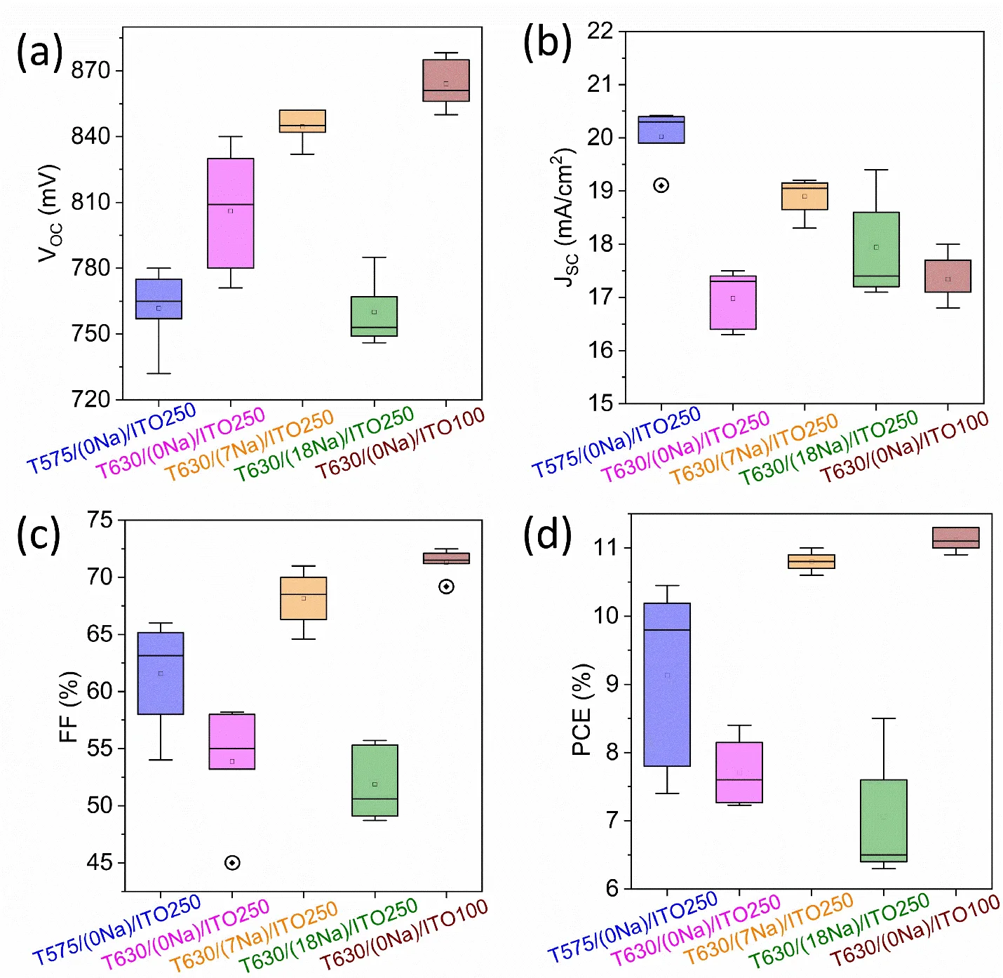
A solar cell usually catches light with one side, and at the back it has a solid metal substrate. Here, the back wall was made from a transparent conducting material — indium tin oxide. Light that the cell doesn't absorb passes through. Such a cell can be placed as the second from the top: the first one takes the blue part of the spectrum, and the lower one takes the red, like two sieves placed one after another.
The cell material is a compound of copper, indium, gallium, and sulfur. Its bandgap (the distance an electron must jump to create a current) is 1.6 electronvolts. This is just right for the top floor: it is transparent to red light but captures blue well. To make the cell work better, sodium is added — the same element found in table salt. Sodium fills defects in the crystal, like putty fills cracks in a wall, and current flows more freely.
At a high growth temperature (630 degrees Celsius), crystals come out more uniform, and the cell glows under ultraviolet light a hundred times brighter — meaning less energy is wasted. At the boundary with the transparent contact, a thin layer of gallium oxide forms. It works like polish on wooden furniture: it closes pores and prevents electrons from getting stuck at the edge. But if this layer is too thick, it starts to hinder the current, like a too-thick layer of varnish prevents opening a drawer. The thin back contact solves this problem.
Original abstract
as written by the authors arXiv:2604.05837
Wide-gap Cu(In,Ga)S2 solar cells with In2O3:Sn (ITO) as transparent back contact are evaluated for the application as top cells in tandem devices. The effect of Na on the solar cell performance is investigated by supplying additional Na by NaF co-evaporation or exclusively by Na diffusion from glass. An efficiency of 12.7% is achieved for a semitransparent solar cell with a band gap of 1.6 eV, with sufficient Na diffusion from glass only, allowed by a thin ITO layer. Absorber grown with additional NaF co-evaporation during Cu(In,Ga)S2 growth on thicker ITO show a comparable efficiency of 12%. High temperature growth at Tsub = 630{\deg}C enhances overall absorber quality and results in wide-gap absorbers, with photoluminescence quantum yield improved to 1.5 x 10⁻⁵, two orders of magnitude higher than absorber grown at low temperature. NaF co-evaporation is effective in suppressing deep defects, thereby reducing non-radiative recombination and enhancing photoluminescence quantum yield further. A GaOx interfacial layer is formed at the rear contact, likely contributing to the passivation of the back contact. With the presence of thick GaOx layer, current blocking effects are visible in the current-voltage curves. On the contrary, a thinner ITO tends to result in thinner GaOx layer and no current blocking is observed.
Indium tin oxide is the same transparent conductor used in smartphone screens: it conducts electricity but doesn't block the view of the picture.