Traps at the Interface: How Defects Mess with Quantum Chips express
A quantum chip is like a musical instrument that goes out of tune at the slightest touch. In devices made from strained germanium, a material where atoms are slightly stretched for better conductivity, the main source of off-key notes is defects at the interface between the semiconductor and the insulating layer. These defects act like microscopic Velcro: they snag charges and prevent them from moving smoothly.
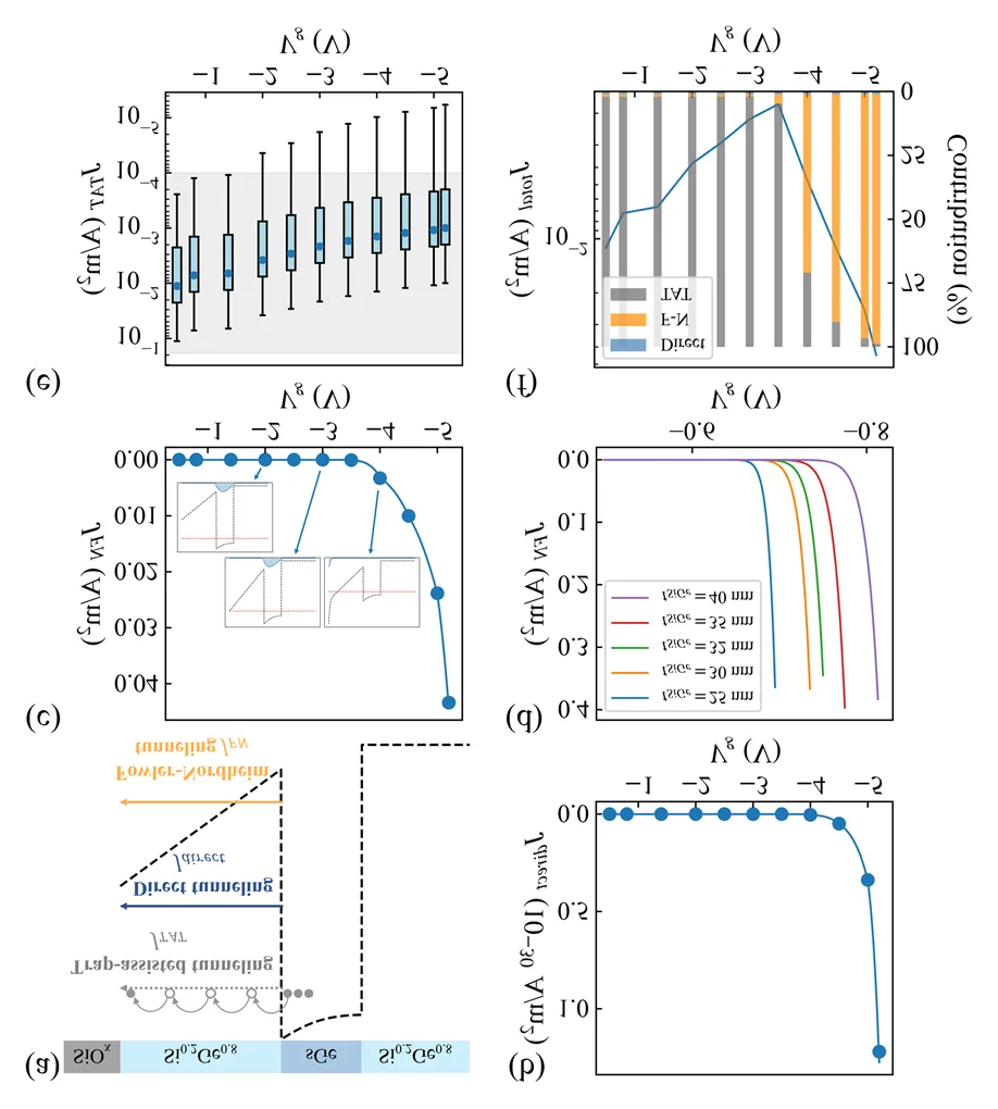
The authors built field-effect transistors (voltage-controlled current switches) based on germanium and silicon. They cooled the samples to cryogenic temperatures (below -200°C) and watched how the traps filled over time. It turned out the process is gradual, like water slowly seeping into a sponge. Then, using a computer model, they calculated exactly how charges tunnel (leak through a barrier) from the active layer to the defects.
They found that at different gate voltages (on the control electrode), two different mechanisms drive the leakage current. At low fields, charges hop through defects like stepping stones across a swamp. At high fields, they punch through the barrier directly, like a powerful stream breaching a dam. This refines the previous picture, which considered only one leakage path.
The practical takeaway: to make germanium quantum devices stable, you need to reduce the number of defects. The authors suggest improving the crystal quality of the barrier layers and lowering dislocation density (structural defects). That way, there will be fewer traps, and the chip will hold its tune longer, like a well-calibrated instrument.
A single square centimeter of the interface between a semiconductor and an insulator can contain billions of trap defects — imagine a pothole on every millimeter of a road.