Holey Film Cools Silicon express
A crowd on a narrow street moves slowly because people bump into each other. In silicon, heat is carried by similar 'shoves'—atomic vibrations called phonons. If you cut tiny holes in a silicon film, phonons will bump into them like pedestrians into lampposts, and heat will flow worse.
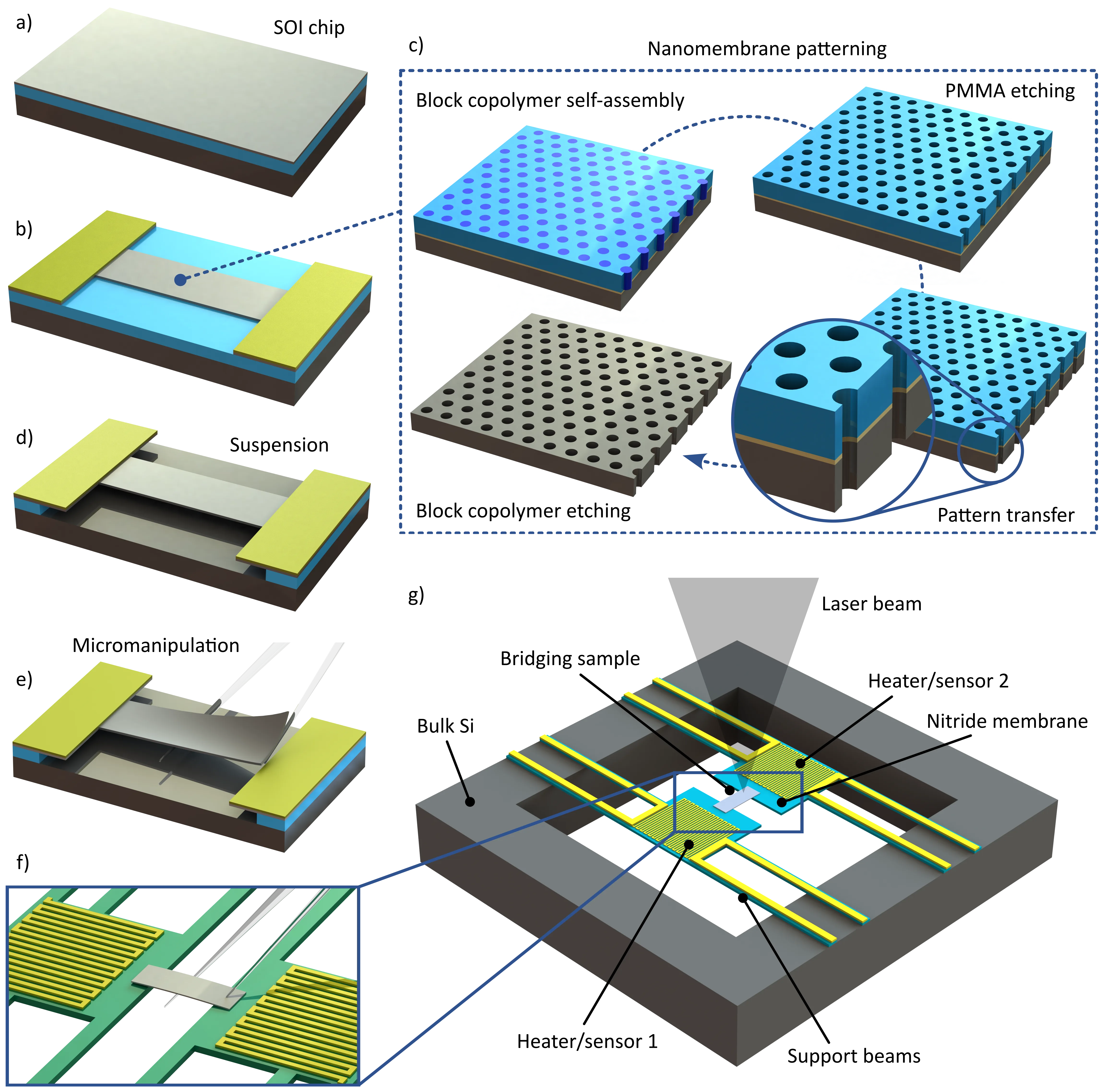
That's exactly what the scientists did: in a silicon film 40 nanometers thick (a thousand times thinner than a human hair), they made holes 35 nanometers in diameter, spaced 63 nanometers apart. The holes are arranged neatly, like a honeycomb, because they were 'drawn' by a self-assembling polymer — long molecules that arrange themselves into a pattern on their own. Then the silicon was etched away following that pattern.
The key trick is the depth of the holes. You can change it without touching either the diameter or the spacing. Fully through-holes block heat the most, while shallow ones block it less. This gives you a 'volume knob' for heat flow: turn the depth, and you change the thermal conductivity.
To accurately measure how much heat passes through such a film, the old three-probe method had to be improved. Usually, the contacts between the film and the substrate get in the way: they add extra resistance, like bad doors in the path of a crowd. The new method accounts for these 'doors' and gives an honest value.
The result is a simple, controllable technology: holey silicon can be tuned for different tasks, from cooling microchips to thermoelectric generators that turn temperature differences into electricity. A street with obstacles turned out to be useful.
Original abstract
as written by the authors arXiv:2604.14770
Phononic silicon structures have emerged as an integrable and scalable nanosystem for tailoring thermal transport. However, their widespread adoption has been limited by their complex fabrication pathways. Alongside, the reliable characterization of thermal properties in suspended nanostructured films remains challenging, as thermal contact resistances often hinder the accuracy of measurements. In this work, we demonstrate a clear and controllable reduction of thermal conductivity in nanopatterned silicon membranes. A block copolymer self-assembly approach is employed to fabricate nanoholed silicon films with a pitch of 63 nm and hole diameters of 35 nm. Additionally, we introduce an extension of the three-probe technique that enables robust, quantitative, and spatially resolved thermal conductivity measurements in complex thin-film systems, accounting for thermal contact artifacts. The method is validated through measurements on unpatterned 40 nm-thick silicon thin films between 30 and 350 K, yielding a room-temperature thermal conductivity of 46.5 W/m.K. Finally, we further show that controlled etching of the nanoholes provides a powerful means to tune thermal transport in the overall studied temperature range, establishing hole etch depth control as an effective parameter in phononic silicon. Specifically, a fivefold reduction in thermal conductivity is achieved, reaching 7.3 W/m.K for fully etched-through membranes at room temperature.
The holes in silicon aren't drilled: they're made using a polymer that self-assembles into a hexagonal pattern, like a honeycomb, only a thousand times finer.