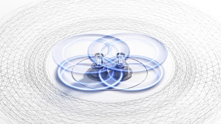
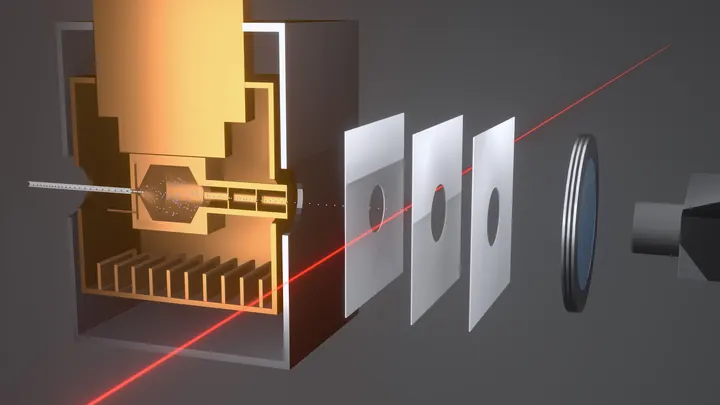
A nanophotonic device is an engineered structure at the nanometer scale that controls light in ways not possible with conventional optics. By patterning materials with features smaller than the wavelength of light, these devices can guide, confine, filter, or enhance electromagnetic fields, enabling ultra-compact components for computing, sensing, and communication. They are central to modern photonic circuits, where they replace bulky lenses and prisms with chip-scale elements that manipulate photons as precisely as transistors control electrons.
History
The field emerged in the late 1980s with the concept of photonic crystals proposed by Eli Yablonovitch and Sajeev John, and expanded with the development of plasmonics and metamaterials in the 1990s–2000s.
How it works
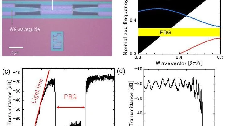
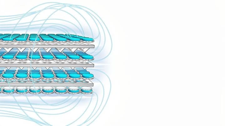
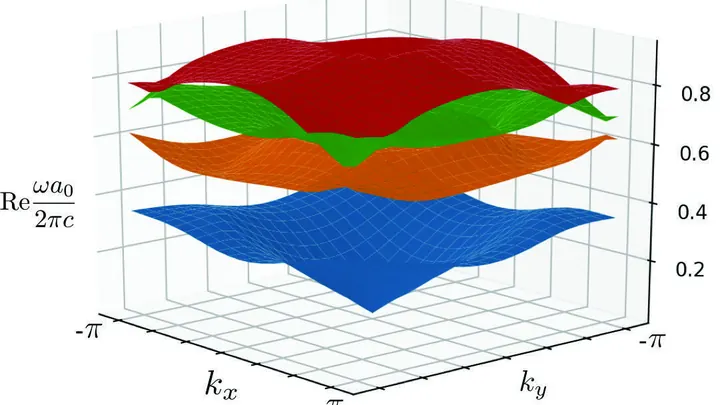
Nanophotonic devices exploit phenomena like photonic bandgaps, plasmonics, or optical resonances. For example, a photonic crystal is a periodic array of dielectric nanostructures that creates a 'bandgap'—a range of wavelengths that cannot propagate, effectively trapping or steering light. Alternatively, metallic nanostructures support surface plasmons, collective electron oscillations that squeeze light into volumes far below the diffraction limit, enhancing light-matter interactions for sensing or nonlinear effects.
In practice
Nanophotonic devices are used in fiber-optic communication components, biosensors for medical diagnostics, and quantum processors where they route single photons between qubits.
Fun fact
Some nanophotonic devices can slow light to a fraction of its vacuum speed, storing it temporarily in a tiny chip.
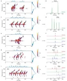
A conductor raises the baton, and the orchestra produces not just sound but a complex score: each note sounds at its own moment, at its own pitch, with the right volume. Light can also be a score, if you control its spectrum and timing. Previously, this required bulky setups that could not be reconfigured after assembly.
A librarian in a rare-book archive takes a volume from the shelf and puts it back without waking the cat dozing nearby. That is roughly how the new quantum memory works: it catches a photon, tucks it into the mechanical vibration of a tiny silicon bridge, and returns it on request.
A tiny diamond, invisible to the naked eye, sits on a chip and senses heat like no ordinary thermometer can. Hidden inside it are two defects: places where a carbon atom is replaced by a nitrogen atom, with a vacancy nearby.
When an alpha particle tears through a gas, it leaves behind not a continuous track but a chain of individual ionizations: tiny flashes where electrons are knocked off atoms. In a living cell, such flashes damage DNA, and the denser they are packed into a clump, the more severe the damage.
Light passing by a tiny structure changes direction. If the structure is smaller than the wavelength of the light, it acts like a lens and focuses the light into a spot smaller than the wave itself.
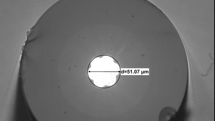
Light in an optical fiber is like a stream: it flows inside a glass thread and doesn't spill out. A thick thread carries many streams at once, a thin one only one. Astronomers often need to pour light from a thick fiber into several thin ones to split it into colors.
You can make light turn on command, like water in a hose — if you know where to squeeze. That's what electro-optic circuits do: they change the direction of a beam inside a chip using an electric field. The classic material for such tricks is lithium niobate, a crystal that responds to voltage like a string to a pluck.
A smartphone camera captures light with tiny sensors, but by themselves, they can't distinguish colors. So color filters are placed in front of them: red, green, blue, like stained glass in a window. Each sensor sees only its own color, and then software assembles the full picture from these pieces.
In an ordinary room, light vanishes the moment you switch off the lamp. In a tiny silicon nitride cavity, a photon can bounce between the walls 80,000 times before it gets lost. It's like a ball thrown into a room that rebounds off the walls with almost no loss of speed.
A light beam usually travels in a straight line, but you can make it spin around its axis, like water swirling into a vortex as it drains. This 'twisted' light carries more information and is needed for ultra-fast communication and quantum computing.
A stack of playing cards lies still. You can slide the top card with your finger: that's crude intervention. Or you can blow so that the whole stack momentarily changes shape, but the cards don't scatter. That's roughly how light, in a new experiment, rearranges a crystal of tin selenide (SnSe).
Usually, to change the structure of a solid, you heat it or pass a current through it.
The orchestra plays, but the conductor hears only a general hum. Each instrument plays its own part, but you can't tell where the flute is and where the double bass is. You need a spectrum analyzer — a device that breaks down sound by frequency.
An empty resonator isn't truly empty. Even in an absolute vacuum, where not a single photon exists, quantum fluctuations persist. They resemble ripples on water in a dead calm: the surface appears smooth, but molecules keep jittering. Physicists have learned to turn this jitter into real waves.
Every night, hundreds of observatories scan the sky, yet planets around other stars remain ghosts. Their light is billions of times fainter than the glare of their parent star — the task seems hopeless. But optics found a way: rather than block the star’s light, cancel it with a counter-wave of the same amplitude, shifted by half a period.
A night river is dotted with tiny sparks. This isn't plankton: it's functional pollen-sensors, millimeter-sized devices that swim on their own and measure the water's chemistry.
Each particle is a tiny lab. Inside, two reagents meet: one triggers a glow upon contact with a pollutant, and the second, a colored filter, blocks out interference.
Organic light-emitting materials are like a busy intersection without traffic lights. Molecules receive energy but, instead of honestly giving it back as light, they often turn into dead ends: they form dark pairs (exciplexes — short-lived complexes that do not emit) or collide with each other, losing charge.
A protein in a cell is not a frozen sculpture but a restless mechanism. Its parts are constantly vibrating, and these movements determine how it grabs molecules, transmits signals, or builds the cellular scaffold. But filming the life of a single protein was hampered by two nuisances at once. First, the movements last millionths of a second — ordinary cameras simply cannot catch them.
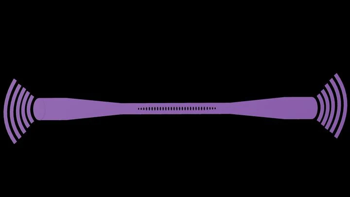
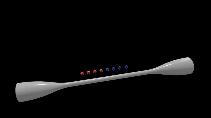
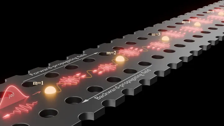
An orchestra without a conductor, where musicians hear each other through a shared wall. That's roughly how the new type of laser works: a few atoms (emitters) sit along a waveguide — a thin track for light on a chip. Light from each atom runs along this track and affects its neighbors.
A typical laser is a cavity where light bounces between mirrors and gets amplified. But you can ditch the mirrors and make light circulate inside a tiny particle smaller than the light wave itself. That's how the new lasers work: nanoparticles of indium phosphide sitting on perfectly smooth gold.
Light flows like an invisible river. If you place an obstacle in the stream, the water whirls into eddies. Likewise, specially designed surfaces create light 'whirlpools' that catch nanoparticles like wood chips.
The thinner the ferroelectric film, the stronger the depolarizing field — a dictate of classical physics. Imagine a pencil balancing on a fingertip: the shorter it is, the harder to keep it upright. Nanoscale polarization likewise strives to vanish.
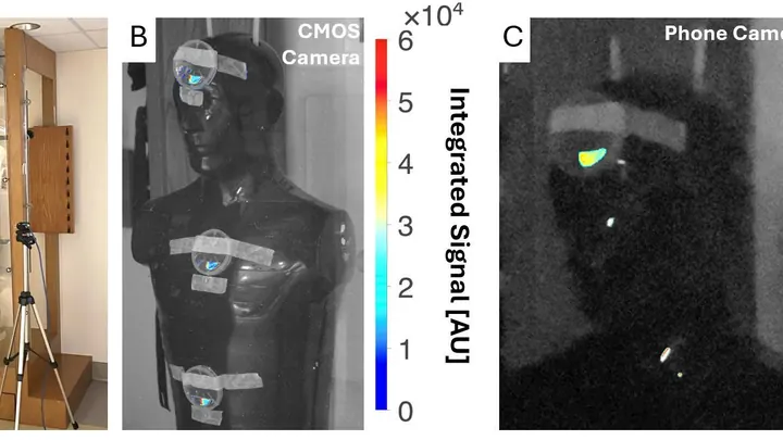
A crystal the size of a matchbox was placed under the beam of a clinical accelerator. Half of its surface was covered with a pattern of nanoscale bumps — tiny, smaller than the wavelength of light. The other half was left smooth. The difference was striking: the coated part produced a signal 4.1 times brighter.
Magnetic particles are attached to the surface of the diamond by DNA strands, like puppets on strings. They constantly dance under the thermal motion of the liquid molecules. The liquid's viscosity sets the pace: in honey, the particles barely tremble; in alcohol, they dance quickly.
Two white sheets lie in the sun — one rough, one smooth. Which one heats up less? The rough one scatters light more strongly, so it seems it would stay cooler. But if the coating is made of many transparent glass beads, the logic changes. Light wanders through it like in a thick fog, and at some point it stops noticing individual droplets.
A smartphone camera captures everything indiscriminately, but the eye immediately picks out what matters. The retina doesn't just pass the image to the brain: it highlights contours on the spot, suppresses noise, and adjusts to brightness.
Quantum bits (qubits) are like delicate music in a noisy factory. Ambient magnetic fields constantly 'drown out' their quantum state, turning a coherent signal into cacophony. Usually, this destructive process is slowed by retuning the qubits themselves to different frequencies, but that doesn't always work.
Light is a stream of photons. In a special waveguide, resembling a narrow corridor, a 'gatekeeper' atom usually lets them through one at a time. This phenomenon is the domain of single-particle spectroscopy.
A flashlight beam aimed through frosted glass turns into a blurry spot with every extra millimeter of thickness. Scintillators, materials that convert X-rays into visible light, behave much the same way. They underpin medical imaging, baggage screening, and detectors at particle accelerators.
A solar telescope is like an eye trying to spot an ant through a pot of boiling soup. The daytime sky dazzles, the air shimmers, and the image swims. To freeze it, you need adaptive optics — a system that predicts distortions and corrects them hundreds of times per second.
Light needs space. A camera lens sits several centimeters from the sensor so the rays have room to focus. Now, that gap has been squeezed to the thickness of a sheet of paper, and light still behaves as if it had traveled its rightful centimeters. That's what 'spaceplates' do: flat elements that mimic free-space propagation.
Any light measurement runs into a fundamental limit: photons hit the camera sensor unevenly. This natural ripple (shot noise) blurs fine details, like trying to pick out a quiet instrument in an orchestra through the noise of the hall.
Two musicians in separate rooms play the same note. The sound must be so identical that a listener can't tell who is playing. In the quantum world, these musicians are single-photon sources — particles of light that must be indistinguishable from one another.
Light, discovered by Maxwell, behaves differently in different media. In a new study, researchers simulated a two-dimensional crystal that absorbs light and has magnetic properties. In it, light waves behave like passengers on a one-way escalator: they relentlessly move toward edges and corners, where they accumulate.
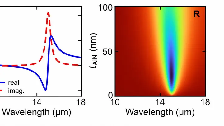
A film of aluminum nitride, as thin as a soap bubble, hangs above a mirror with a micrometer-sized air gap between them. When invisible infrared light with a wavelength of about 15 micrometers hits it, the film starts to vibrate in sync with the light, like a string that responds only to its own note.
The nucleus of a thorium-229 atom is like a taut guitar string: it vibrates at a strictly defined frequency. To 'pluck the string', a precise strike is needed — a laser beam of a very specific color.
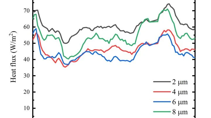
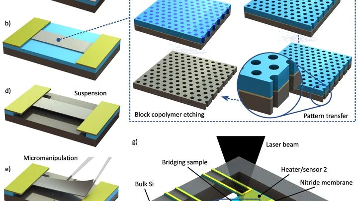
A crowd on a narrow street moves slowly because people bump into each other. In silicon, heat is carried by similar 'shoves'—atomic vibrations called phonons. If you cut tiny holes in a silicon film, phonons will bump into them like pedestrians into lampposts, and heat will flow worse.
Ordinary light scatters in all directions, like water from a shattered glass. But in some crystals, light waves can bunch together into narrow beams and flow in a single direction, like water in a trough. Physicists studied such a material: layered vanadium oxide α-V2O5.
In this crystal, atoms vibrate differently along and across the layers.
Conventional photolithography, used to make chips, hits a fundamental limit: light cannot draw features smaller than its wavelength. Here, they took a different route. First, they made sparse vertical ridges of oxide, then deposited layers of aluminum oxide, each one atom thick, onto them.
Imagine trying to examine a snowflake without letting it melt or get damaged. That's roughly the challenge facing scientists who want to study individual proteins — the tiny molecular machines of life. In solution, a protein constantly jiggles and clumps with its neighbors, and in an electron microscope, the beam destroys it.
An ordinary lens always refracts light the same way. Its properties are frozen in glass forever. But now there's a surface that changes the game on the fly.
Scientists made an ultrathin film with resonant elements and infused it with liquid crystals — the same stuff used in phone screens.