The Light Chip: A Treasure Map in a Sea of Chaos express
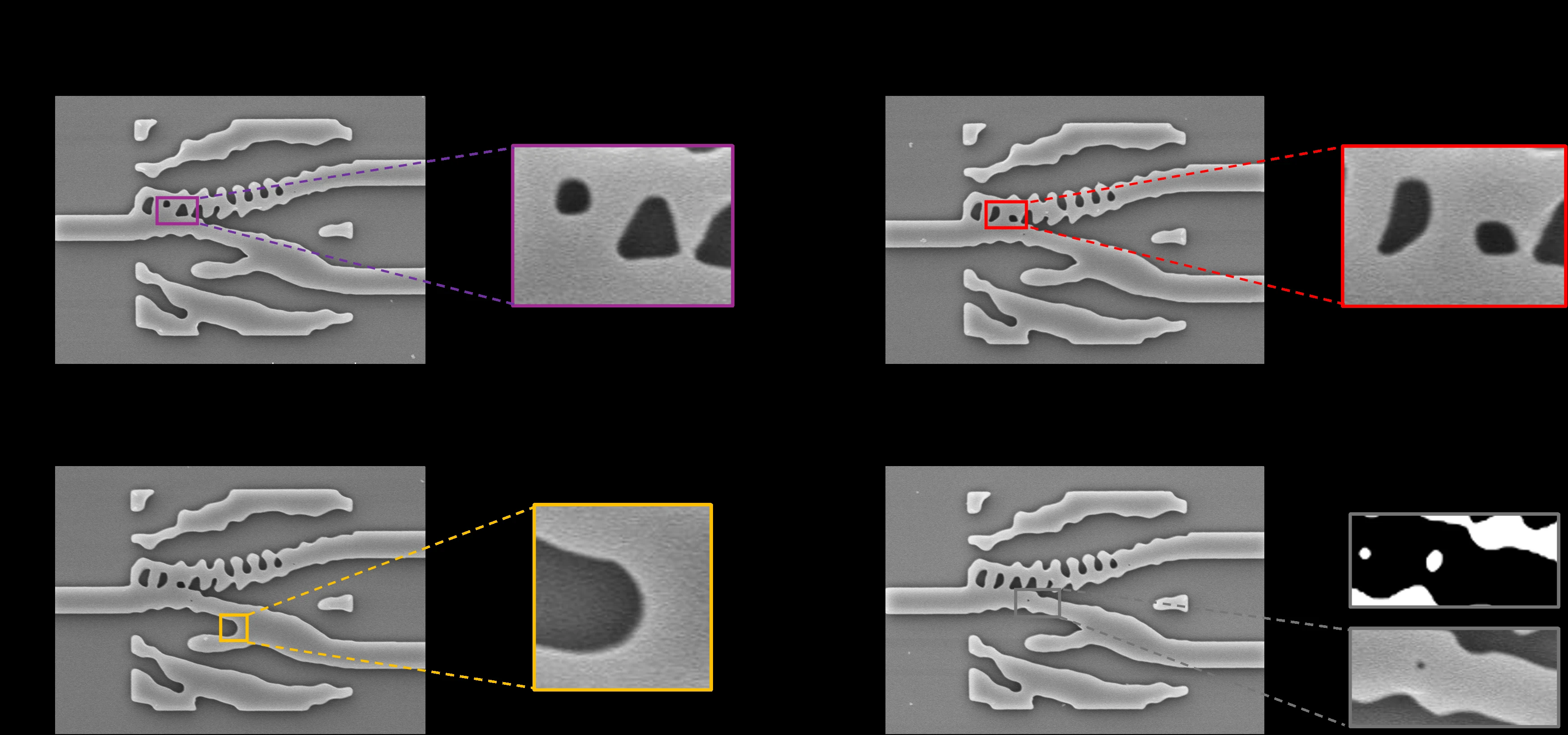
Computer algorithms design light chips that separate signals by color not along straight lines but through mysterious, winding mazes. These chaotic, almost organic patterns work brilliantly, but until now, no one knew which parts of the design truly mattered. The slightest manufacturing deviation could cripple the device, yet engineers couldn't predict where it would be fatal.
Scientists found a solution: an additional AI draws a sensitivity map over the blueprint. Bright spots on it, like marks on a treasure map or hidden reefs, point to areas where any inaccuracy is catastrophic. Real-world chip tests confirmed: damaging a "hot" spot increases signal loss by 11 times more than wrecking an unimportant zone.
This method doesn't require changing complex computer models: it just adds clarity. Designers can now see in advance whether a circuit will survive inevitable manufacturing imperfections. In the future, this will speed up the production of reliable light chips for next-generation internet or quantum computers.
Original abstract
as written by the authors arXiv:2510.22176
As an increasingly powerful technique in integrated photonics, inverse design uses optimization algorithms to automatically create compact, high-performance photonic structures, often yielding non-intuitive layouts far more compact than conventional designs. While adjoint-based inverse design is a prominent optimization method, the resulting free-form layouts are difficult to interpret or diagnose under fabrication variability, even for experienced photonic device designers. We present an experimentally validated interpretability workflow that produces pixel-level sensitivity maps directly on the binary mask of an inverse-designed device. Using wavelength-division demultiplexers (WDMs) at 1310/1550 nm as examples, we train a lightweight convolutional surrogate to regress figures of merit (FoMs) and apply Integrated Gradients (IG) to attribute predicted transmission to individual pixels. We demonstrate that high-attribution hotspots correspond to physically meaningful substructures, such as splitter hubs and high-curvature edges. Experimental results show that controlled perturbations in these high-sensitivity regions result in up to an 11x higher excess insertion loss compared to perturbations in non-sensitive regions, consistent with full-wave simulations. This approach adds a practical explainability layer to existing pipelines, offering a clear pathway for foundry-compatible design-rule checking and fabrication-aware constraint allocation without modifying the underlying electromagnetic solver.
Many computer-generated designs surprisingly resemble biological forms: whimsical curves that look like coral or blood vessels, yet they obey strict physical laws.
In science fiction, AI spawns blueprints that defy human logic; now we have a key to decipher them.