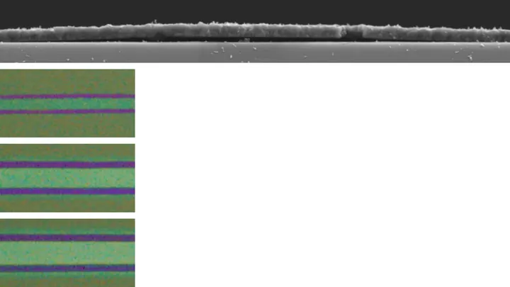
Lithography is the core patterning technique in microfabrication, used to transfer geometric shapes onto a thin film or substrate. It is the reason modern microchips, sensors, and photonic devices can pack billions of features onto a single chip. The process works by coating a surface with a light-sensitive material (a resist), exposing selected areas to radiation (usually ultraviolet light, but also electron beams or X-rays), and then chemically developing the resist to leave a mask. This mask protects parts of the underlying layer during etching or deposition, so the pattern is physically carved into the material.
History
The technique evolved from photolithography used in printing and was adapted for semiconductor manufacturing in the late 1950s, notably by Jay Lathrop and James Nall at the U.S. Army's Diamond Ordnance Fuze Laboratories in 1957.
How it works
The essential mechanism is selective exposure. A mask or a scanned beam defines which regions of the resist are altered. In optical lithography, light passes through a photomask, projecting a pattern onto the resist; in electron-beam lithography, a focused beam writes the pattern directly. After development, the resist acts as a stencil: areas left exposed are removed or hardened, depending on the resist type. Subsequent steps—etching, ion implantation, or thin-film growth—transfer the pattern into the functional material. The resolution limit is set by the wavelength of the radiation and the optics, which is why advanced methods use extreme ultraviolet light or electron beams.
In practice
Lithography is used to fabricate integrated circuits, microelectromechanical systems (MEMS), photonic chips, and even microfluidic channels for lab-on-a-chip devices.
Fun fact
Modern extreme ultraviolet lithography uses light with a wavelength of 13.5 nanometers—about 40 times shorter than visible light—and requires mirrors coated with molybdenum/silicon multilayers because no lens can focus that radiation.
A globe sits on a table, and a ruler lies beside it: one is curved, the other straight. X-ray telescopes have lived with this mismatch for years. Their mirrors gather light onto a curved surface, like the globe, while the detectors that catch that light have been flat, like the ruler.
A sheet of paper left on a wet table warps and lifts its edges. No one controls that motion, but it follows the same laws as plant growth: some areas of the sheet shrink more than others, and the flat form becomes three-dimensional. Engineers have long dreamed of taming this process so that a flat blank folds itself into a desired sculpture. In the new work, that trick succeeded with accuracy down to one percent.
A deck of cards in which each card is slightly rotated cannot lie flat: the backs and faces will never align. But if the cards are flexible, they will start to adjust, shifting by fractions of a millimeter to find the perfect match. Something similar happens inside crystals when two thick layers of MoS2 or MoS2 with WS2 are stacked with a twist of 1–2 degrees.
Space construction today is a costly hassle with prefabricated parts: every panel has to be lifted from Earth, then assembled in zero gravity, like building a model kit while wearing thick gloves. Engineers from a new study propose a different path: not hauling or printing, but letting the liquid itself sculpt the structure.
When light hits ordinary plastic, some of it reflects, like a glare on a window. To eliminate this glare, a special coating made of tiny structures is applied to the surface, which cancels out the reflection.
A superconducting quantum interferometer is a device that senses magnetic fields billions of times weaker than the needle of an ordinary compass. Inside it, there is a narrow bridge where superconductivity briefly breaks.
You can make light turn on command, like water in a hose — if you know where to squeeze. That's what electro-optic circuits do: they change the direction of a beam inside a chip using an electric field. The classic material for such tricks is lithium niobate, a crystal that responds to voltage like a string to a pluck.
Imagine a multilayered shell where metal and insulator layers alternate like pages in a book. Such a structure can make an object hidden inside invisible to an observer. Light bends around it as water smoothly flows around a smooth stone: no ripple, no splash — no reflection, no shadow.
If you clap your hands in an empty room, the echo will tell you about its size and shape. Every object (a chair, a book, a person) adds its own signature to this echo: sound reflects off it in a particular way. The authors of the paper have figured out how to completely rewrite this acoustic signature. They surrounded a region of space with a closed surface of microphones and loudspeakers.
Two white sheets lie in the sun — one rough, one smooth. Which one heats up less? The rough one scatters light more strongly, so it seems it would stay cooler. But if the coating is made of many transparent glass beads, the logic changes. Light wanders through it like in a thick fog, and at some point it stops noticing individual droplets.
A bridge of aluminum just a few atoms thick is the heart of many quantum devices. Current flows through such a bridge without resistance, and it can be controlled with a magnetic field. These bridges are called Josephson junctions, after the British physicist who described their behavior.
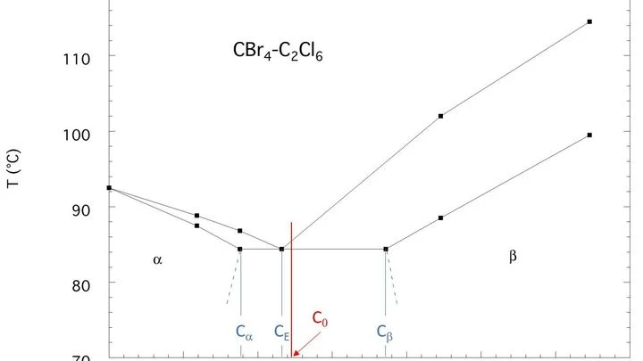
In a solid piece of tin-lead alloy, the layers of the two metals lie like pages in a book. When heated from one side, the layers don't melt uniformly but in whimsical tongues and fingers. Scientists studied this process using a transparent alloy that can be seen through under a microscope and compared it with a computer model.
Conventional photolithography, used to make chips, hits a fundamental limit: light cannot draw features smaller than its wavelength. Here, they took a different route. First, they made sparse vertical ridges of oxide, then deposited layers of aluminum oxide, each one atom thick, onto them.
When light passes through a turbid medium, like a glass of milk or frosted glass, it scatters in all directions. But sometimes, instead of spreading out, it gets trapped in tiny 'pockets' inside the material. Physicists call these pockets localized modes: light falls into them as if into a trap and cannot escape.
Think of a stack of paper: when the sheets lie perfectly aligned, light passes through them uniformly. But turn one sheet by a few degrees, and the picture changes. Something similar happens with layers in certain materials: rotate them relative to each other, and their properties change — sometimes dramatically.
Spectroscopy isn't the key here, or rather, it's not the method used.
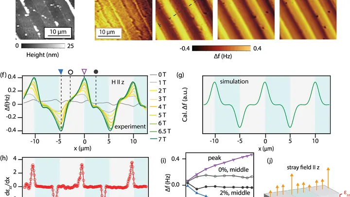
On the surface of a thin film of bismuth iron oxide, you can see neat stripes, like furrows in a plowed field. What lies beneath them has remained a mystery until now.
An ordinary sheet of paper looks white because it scatters all light rays chaotically. But a butterfly's wing shimmers blue and green without a drop of paint: its surface is covered with microscopic grooves that dampen some light waves and amplify others. Engineers have long dreamed of replicating this trick: creating a material that colors itself simply by trapping light in the right places.
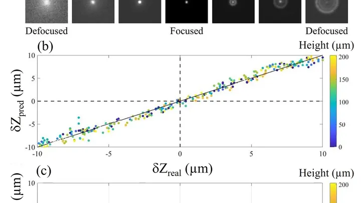
To avoid losing a fast soccer player in the frame, a drone doesn't need a bright beacon — recognizing the silhouette is enough. Similarly, a neural network now tracks microbes: the algorithm analyzes an ordinary microscope image and instantly finds a bacterium in a drop of water.
A laser beam strikes a gold-and-silver film for just a few nanoseconds — in that time, light travels less than a meter. At the point of impact, the metal boils, splatters, and freezes into a random pattern of tiny particles. Each pattern is as unique as cracks in ice or tree branches.
Fibers in composites, paper, or biological tissues are often hidden from view, but their orientation determines the strength and properties of the material. Previously, to see fiber directions, you had to take many images at different angles and assemble a three-dimensional picture, like slicing a loaf of bread into thin pieces. For thin samples, this approach doesn't work: you can't slice what isn't thick enough.
Quantum materials are like finicky flowers: they only bloom in the cold. At room temperature, they hide their unusual properties, but when deeply cooled, they become superconductors or change their magnetic behavior. To understand how they work, you need to examine their atoms in the very cold where these properties reside.
A standard MRI machine is a huge magnet that you can't move, plus a powerful computer that turns signals from the body into a picture. In recent years, portable scanners with weaker fields have appeared: they are light, cheap, and can work in a field hospital or an ambulance.
An octopus tentacle bends, grabs, and stretches — all without a single bone. The secret is that inside it, sections that contract alternate with sections that remain passive. Scientists have long tried to replicate this trick in artificial materials, but until now they couldn't precisely dictate how a material would change shape.
Now researchers have proposed 3D-printing elastic threads from two materials at once.
A quantum computer is like a musical instrument: even a tiny scratch on a string ruins the sound. Instead of strings, we have superconducting resonators — thin traces of titanium nitride on a silicon wafer.
A piece of gold doesn't attract paperclips. But if you take a thin film of a gadolinium-gold-germanium alloy and start bending it, magnetic regions can appear. Scientists did this not with their hands, but with a beam of helium ions that penetrated the material through a patterned mask.
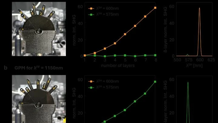
When two light beams meet in a crystal, they can generate a third beam with a different frequency. For this process to be efficient, the waves need to stay in step, like two people walking side by side without breaking stride. Previously, two old tricks were used: either picking a crystal with the right properties, or slicing it into thin layers.
A sheet of graphene is a lattice of carbon atoms arranged like a honeycomb. Electrons in it zip around so fast they seem to have no mass, just like light. When a powerful laser pulse hits such a sheet, the electrons get a kick and start accelerating. Their path can be compared to a road with occasional barriers — the forbidden zones.
A lithium niobate crystal is like a layered cake: inside, electric fields alternate like layers of filling. If you slice such a crystal into thin films and imprint stripes of alternating polarity, you get a periodic structure that makes light change color as it passes through. This is how pairs of photons are born, entangled like twins.
A laser beam passes through glass and touches a thin diamond film. At the point of contact, the film turns into a narrow strip that lifts slightly. We place a second strip next to it, and between them remains an empty corridor. That's the channel: its width can be fifty times its height, like a sheet of paper lying on a table.
A light beam passing through a piece of glass usually just bends slightly. But if you engrave ultra-fine patterns inside the glass with a laser, you can make the light split into separate beams, much like white light fans out into a rainbow after rain.
Terahertz radiation sits between microwaves and infrared light. It passes through clothing, paper, and plastic, but not through metal or water. That's why it's used in security scanners and medical imaging. To see the polarization of such radiation, you need a detector.
Imagine blinds that don't just block or let through light but change its color. Light hits the slanted stripes, and some rays come out a different shade, as if a white beam, passing through the slits, turned green. That's exactly how this new surface works: on a thin film of lithium niobate (a material that can transform light), there are slanted stripes of titanium dioxide.
In winter, puddles freeze, and ice cracks the asphalt. Inside a living cell, freezing does something similar: ice crystals tear its membrane. To prevent this, the cell is soaked in a special solution, like antifreeze for a car. But precision is key: too little solution and ice still forms; too much and the solution itself poisons the cell.
An ordinary laser amplifies light into a bright beam. Run the process in reverse, and you get an anti-laser — a device that sucks in light without a trace. But such a machine is finicky: even a slight disorder can ruin the absorption.
Physicists have found a way to make the anti-laser invulnerable.
A typical 3D printer squeezes out plastic like a pastry chef piping cream from a bag. Here, instead of plastic, it's light. A laser beam draws in liquid resin, making it solidify at precise points. This creates parts too small to see without a microscope.
Until now, such printers were slow: the beam crawled across the surface like a pen on paper.
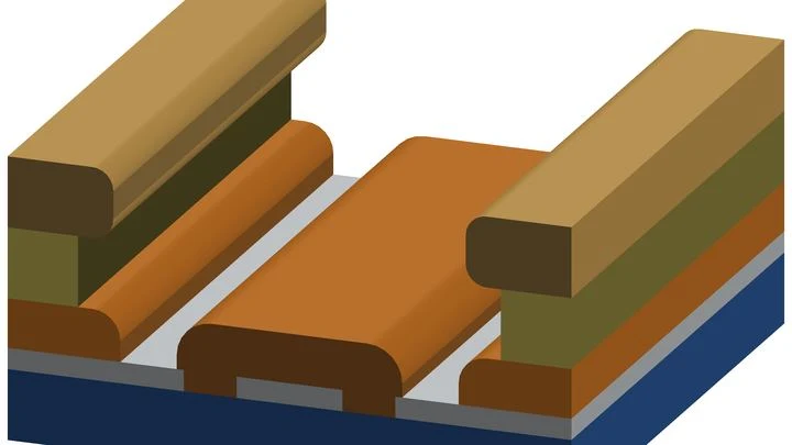
In microchips, wires usually lie flat on the surface, like rails on the ground. But sometimes one wire needs to leap over another without touching it. For that, engineers build air bridges — thin metal arches suspended above the chip.
Previously, such a bridge was assembled in several stages: deposit a layer, expose it, etch it, repeat. Each stage is a chance to mess something up.
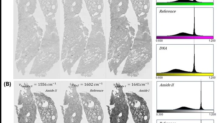
A pathologist looks through the eyepiece and sees a pink-purple tissue section — the classic hematoxylin and eosin stain. The dyes bind to nuclei and cytoplasm, and the color tells the doctor about the disease. But preparing the slide itself takes hours: fixation, paraffin embedding, sectioning, staining.
This new device skips the dye.
A printer that prints not with ink but with metal and ceramic is now a reality. Scientists took an ordinary drop of water containing dissolved metal salts and made it deposit copper, zinc oxide, or nickel hydroxide onto a surface — all with precision down to millionths of a meter.
The secret lies in electricity.
A drop of blood is a bustling city in miniature. Thousands of different molecules scurry through it, each leaving its own trace. But peering directly into this city is hard: the streets are tangled, and there are so many inhabitants that counting them all individually is out of the question.
Scientists have found a way to listen to the whole city at once, without singling out its residents.
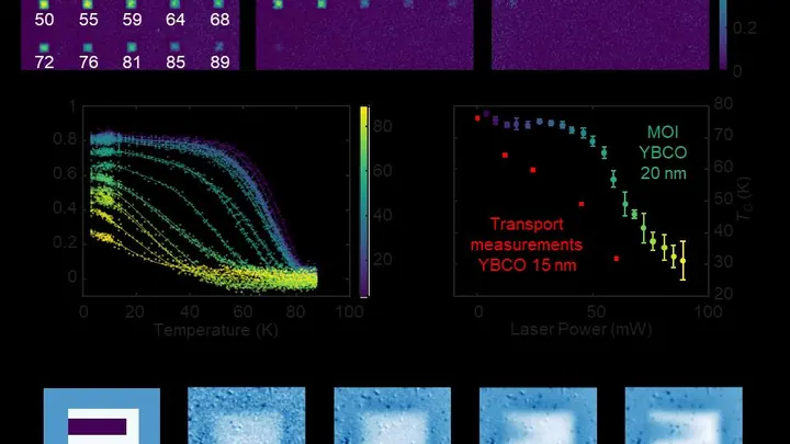
A laser beam, like a fine chisel, burns oxygen out of a superconducting film. Where oxygen becomes scarce, the material stops conducting electricity without resistance. The researchers used this trick to draw patterns on the film that alter its properties.