A Spectral Mosaic in Two Layers express
The glow of an ultrathin sandwich made of two semiconductor layers, molybdenum selenide and tungsten selenide, resembles a tangled musical score: many narrow colored lines that merge into a general background. Figuring out which line comes from where is nearly impossible.
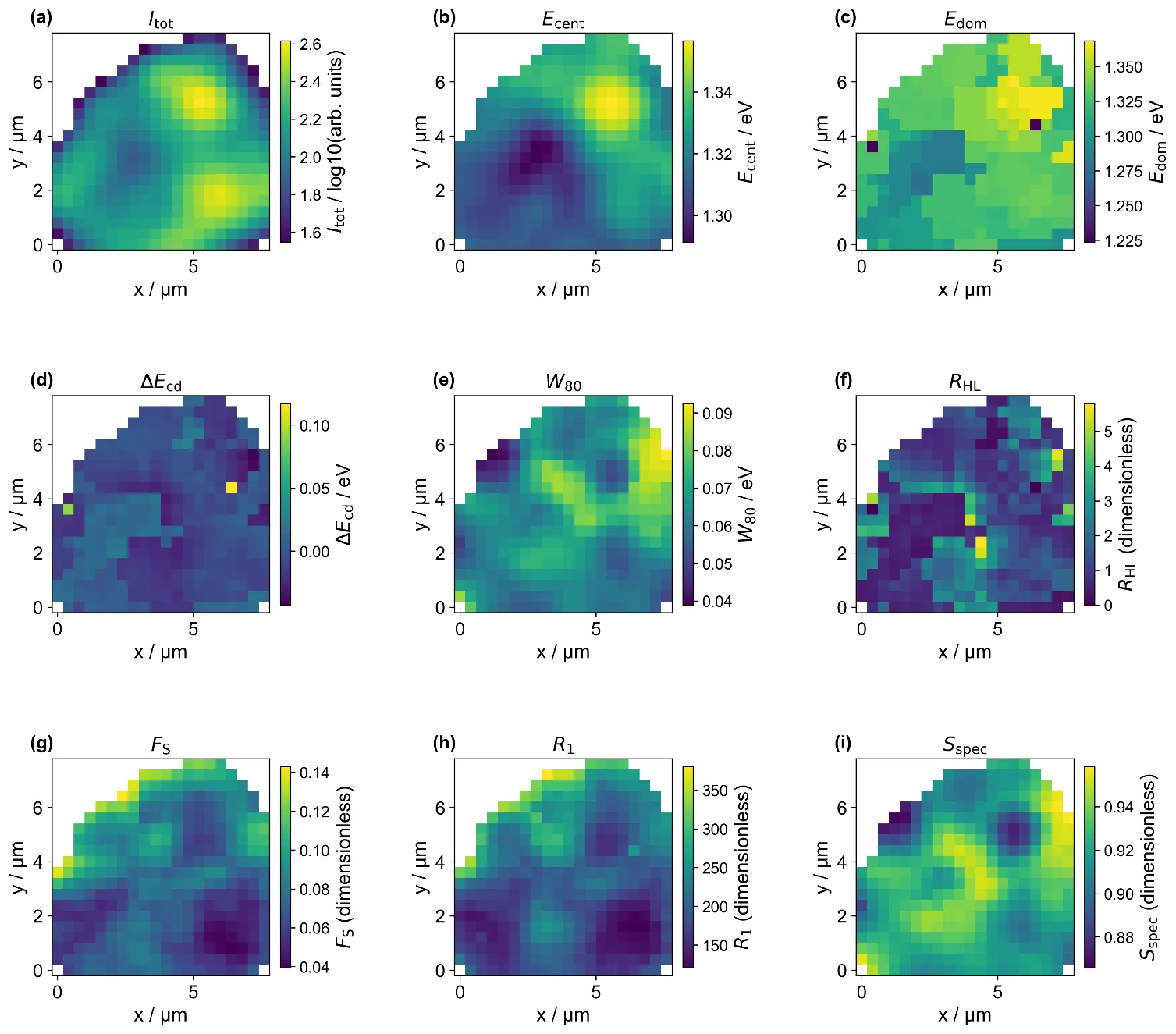
The authors did not try to disentangle the lines one by one. Instead, they mapped the emission with a step of 400 nanometers — hundreds of times thinner than a human hair. It turned out that the entire variety of lines falls into three broad groups, each occupying its own patch of the sample, like a patchwork quilt. These patches range from 1.27 to 2.05 micrometers in size, while the light spot used to illuminate the sample was only 0.85 micrometers across. In other words, each patch is larger than the beam used to examine it.
The researchers measured seven characteristics of the emission: the position of the main line, its width, asymmetry, roughness, and others. They found that the large-scale pattern, the arrangement of patches, and the fine complexity within them are related, but can be studied separately. The authors call this two-level order hierarchical inhomogeneity: first large regions, then fine structure inside.
This result helps understand the structure of so-called moiré superlattices — materials in which two layers are slightly rotated relative to each other, giving rise to a new periodic pattern, like when two combs with different tooth spacings are overlaid. The emission of such materials is important for future ultrathin light sources and quantum devices, where precise control of each photon is needed.
The moiré pattern gets its name from moiré silk, a fabric whose interlaced threads create shimmering waves. In physics, the same effect occurs when two grids with slightly different spacings are overlaid, and it generates new, much larger periods.