Quantum Sentinel for Power Electronics express
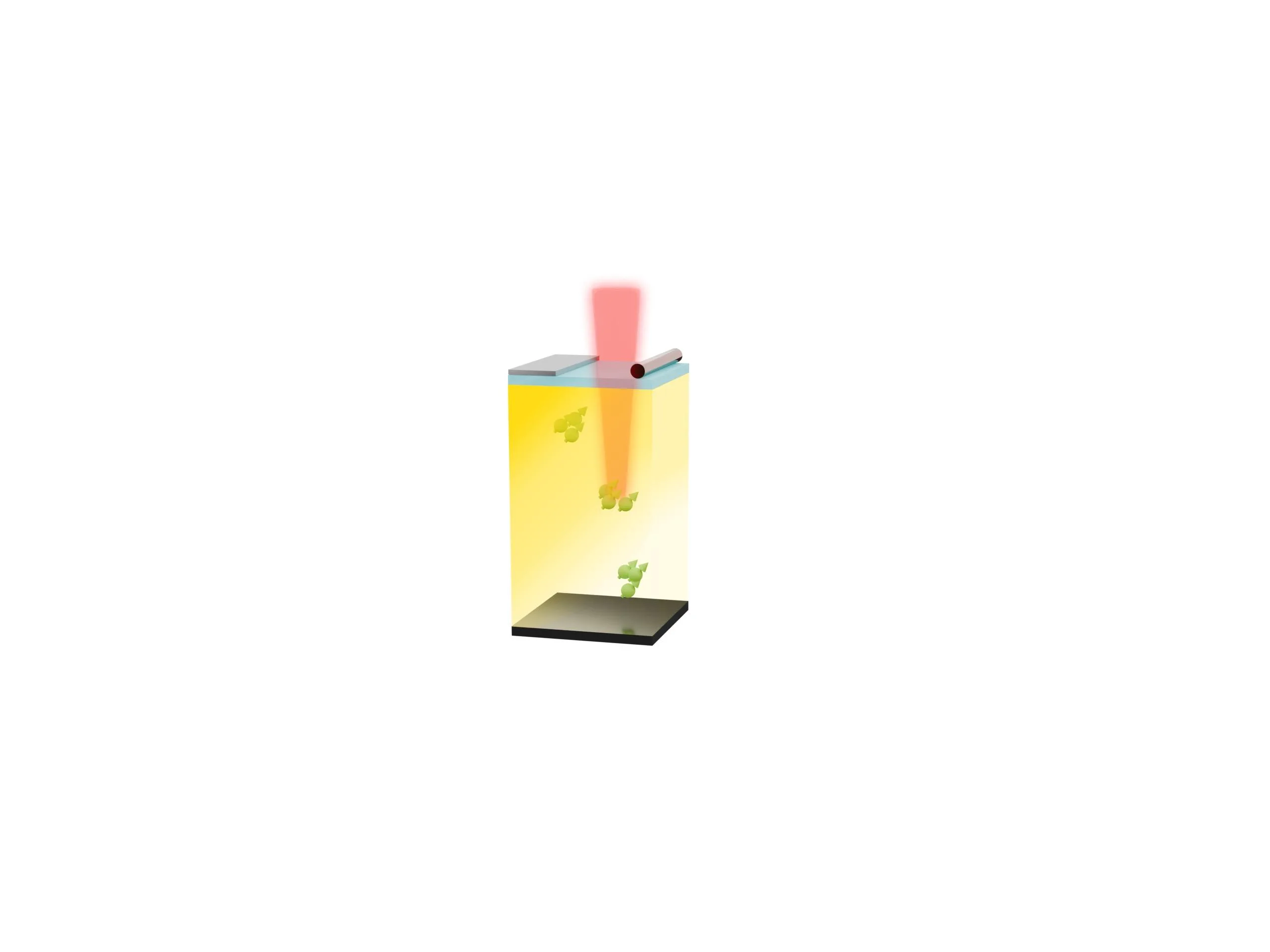
A power transistor made of silicon carbide operates under voltages thousands of times higher than what comes out of a wall outlet. If the field inside it becomes uneven, the device burns out. Previously, this field was invisible: it is too strong for ordinary sensors, and the device must remain under voltage. Now, a tiny spy has been found in the crystal — a defect that glows in response to the field.
This defect is a vacancy where a silicon atom should be. Such a vacancy behaves like a compass needle: its glow changes depending on the direction of the field. Remarkably, the needle senses the field equally well both along and across the crystal. It's like a compass that not only shows north but also altitude. No other sensor does this.
Spectroscopy of the vacancy's glow allows mapping the field inside the device with a resolution of less than a micrometer. You can locate where the field gathers into a dangerous "fist" and redesign the device so that the blow lands on a stronger spot. This approach turns power electronics development from trial and error into an exact science.
A single silicon vacancy in silicon carbide is smaller than one millionth of a millimeter, yet it can report on a field thousands of times stronger than the field inside a thundercloud.