Heat Turned into Light: A Silicon Path to Energy express
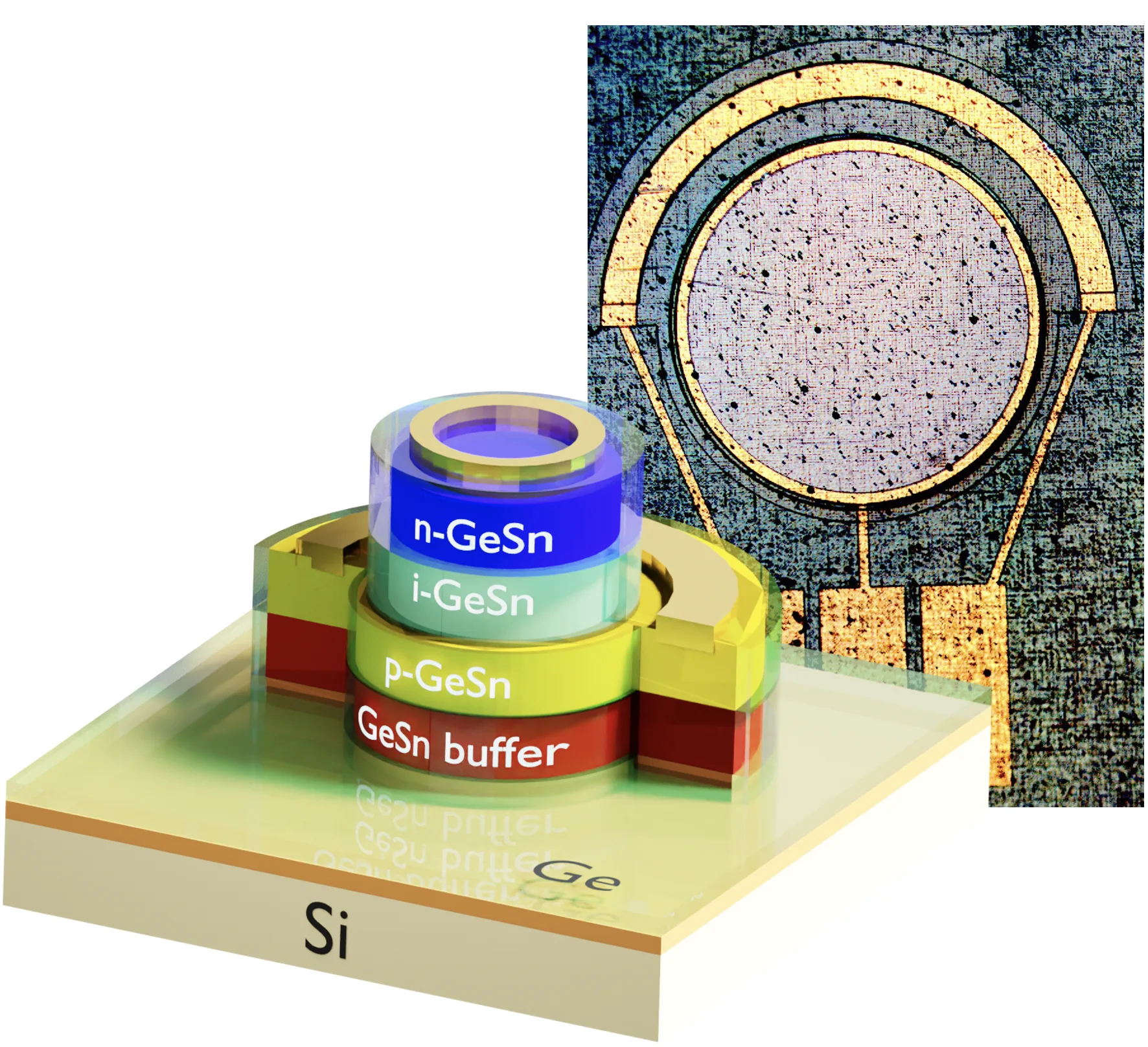
A blazing furnace in a workshop or the hot exhaust of a turbine is not just heat: it's light, invisible to the human eye. Regular solar panels catch visible light, but here you need a receiver for invisible thermal radiation. A team of researchers has, for the first time, built such a receiver from a germanium-tin alloy — a material that can be grown directly on silicon wafers, just like standard computer chips.
They tested a sample the size of a pinhead: they aimed a laser beam with a wavelength of 2.33 microns at it, along with light from a ceramic plate heated to 1500 kelvins. The device produced a current, albeit a modest one — power output was about 0.41 milliwatts per square centimeter. That's hundreds of times less than expensive indium arsenide counterparts, but the key point is: the material works.
Calculations show that the main problem is defects in the crystal, which kill charge carriers along the way. If those are removed, power could rise to 1 watt per square centimeter — thousands of times more. Then such a device could power sensors in factories, in space, or even at home, harvesting heat that today just goes up the chimney.
Original abstract
as written by the authors arXiv:2602.21392
Thermophotovoltaic (TPV) cells are increasingly attractive for applications in industrial waste heat harvesting, aerospace energy management, and compact power generation. Deploying midwave-infrared (MWIR) TPV in practical applications requires narrow-bandgap semiconductors that not only absorb low-energy photons but also integrate with scalable, low-cost platforms. Although high-performance TPV devices have been demonstrated using III-V materials such as InAs, GaSb, and InGaAs(P), their use remains limited by cost and substrate size. With this perspective, narrow bandgap GeSn alloys are a promising alternative that extend group-IV absorption into the MWIR while being silicon-compatible. Although the potential of GeSn TPV cells has been predicted, no experimental demonstration has been reported. Here, proof-of-concept Ge$$_{0.91}$$Sn$$_{0.09}$$ p-i-n TPV diodes (1 mm diameter) grown on silicon were fabricated and their performance was benchmarked against commercial InAs and extended-InGaAs devices. Measurements at 300 K under 2.33 $$\mu$$m laser and $$\sim$$1500 K SiC Globar illumination revealed peak responsivity of $$\sim$$ 0.2 A/W at $$\sim$$ 1.7 $$\mu$$m, and an output power of $$\sim$$ 0.41 mW/cm$$^2$$. These devices show trends comparable to those of the InAs diode under identical conditions, although at reduced absolute levels. To assess the intrinsic performance potential, Poisson-drift-diffusion modeling incorporating experimentally calibrated emitter emissivity predicts power densities exceeding 1 W/cm$$^2$$ under moderate MWIR thermal illumination, indicating that the present devices operate far below their fundamental limits and are primarily constrained by defect-assisted recombination and transport losses. These results establish GeSn as a scalable, silicon-compatible MWIR TPV platform and highlight a larger performance potential achievable through material and device optimization.
The germanium-tin alloy can be applied to silicon like frosting on a cookie, in a thin layer, without cracking.