A silicon wafer is a thin, circular slice of highly pure, single-crystal silicon that serves as the foundational substrate for most modern microelectronics. Nearly all integrated circuits, microprocessors, and memory chips are built on silicon wafers. The wafer's perfect crystalline structure and semiconducting properties allow for the precise fabrication of billions of transistors on a single chip, enabling the digital revolution. Beyond electronics, silicon wafers are also used in photovoltaics, MEMS (microelectromechanical systems), and as optical substrates.
History
The use of silicon as a semiconductor material was pioneered in the 1940s and 1950s, with the first silicon transistor demonstrated in 1954. The development of the planar process by Jean Hoerni in 1959 and the integrated circuit by Robert Noyce and Jack Kilby led to the widespread adoption of silicon wafers.
How it works
Silicon wafers are produced by growing a large single crystal of silicon (via the Czochralski process) and then slicing it into thin discs. The wafers are polished to a mirror finish to create an atomically flat surface. Through photolithography, etching, and doping, intricate patterns of conductive, insulating, and semiconducting regions are created on the wafer's surface, forming the electronic circuits. The wafer acts as both a mechanical support and a semiconductor base, with its electrical properties modified locally to create transistors and other components.
In practice
Silicon wafers are the standard substrate for manufacturing virtually all microchips, from computer processors to sensors in smartphones, as well as for solar cells in photovoltaic panels.
Fun fact
A single modern silicon wafer can contain over 100 billion transistors, more than the number of stars in our galaxy.
A slice of eucalyptus a tenth of a millimeter thick is placed under a polarized light microscope, and the wood suddenly blooms: blue, yellow, and pink bands twist into spirals, forming rings and swirls. This is not paint but the play of light: the cellulose fibers that make up cell walls transmit light differently depending on their orientation.
Space construction today is a costly hassle with prefabricated parts: every panel has to be lifted from Earth, then assembled in zero gravity, like building a model kit while wearing thick gloves. Engineers from a new study propose a different path: not hauling or printing, but letting the liquid itself sculpt the structure.
A single photon is like a perfectly smooth brick from which quantum technologies can be built. But to build a house, you need thousands of identical bricks. Rubidium atoms are natural emitters: each atom emits photons of exactly one wavelength, like a tuning fork that always produces a single note.
A superconducting quantum interferometer is a device that senses magnetic fields billions of times weaker than the needle of an ordinary compass. Inside it, there is a narrow bridge where superconductivity briefly breaks.
Waves on the water's surface usually break against any obstacle — a rock, a piling, an island. But what if you arrange obstacles so cleverly that the wave barely notices them? In a new study, scientists assembled a pattern of many points on the water, arranged according to special mathematical rules, and sent waves through them.
A light beam usually travels in a straight line, but you can make it spin around its axis, like water swirling into a vortex as it drains. This 'twisted' light carries more information and is needed for ultra-fast communication and quantum computing.
The orchestra plays, but the conductor hears only a general hum. Each instrument plays its own part, but you can't tell where the flute is and where the double bass is. You need a spectrum analyzer — a device that breaks down sound by frequency.
Blood vessel cells were seeded onto a transparent film just 700 nanometers thick — a hundred times thinner than a human hair. Flat electrodes are hidden beneath the film. They send a weak alternating current and listen as the resistance changes.
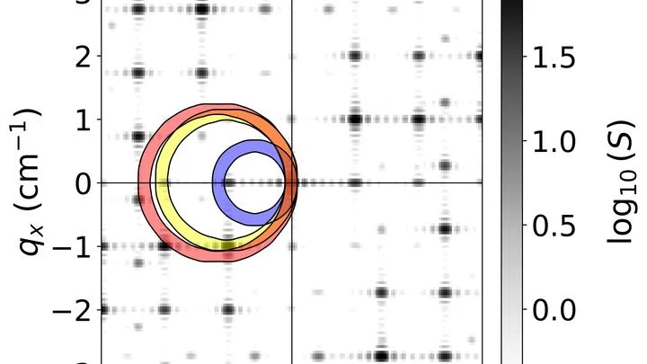
In an ultrathin sheet of four-layer graphene, electrons can behave like a frozen liquid. When cooled strongly and subjected to an electric field, they stop darting around and line up into a regular pattern — a Wigner crystal. It's similar to how water droplets on a frosty morning turn into ice honeycombs.
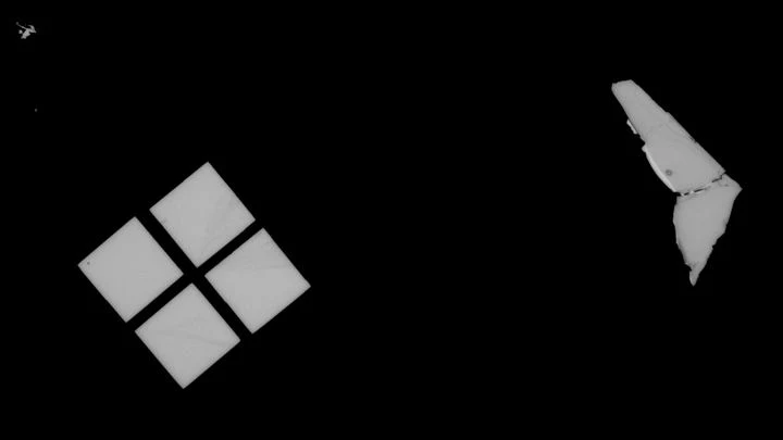
A sugar cube squeezed between your fingers will almost certainly crumble rather than compress evenly. A similar challenge faces quantum computer builders. They need to slightly stretch or compress miniature silicon plates — qubits are later placed on them.
An ordinary field-effect transistor is like a faucet with a very sensitive handle: turn it slightly, and water flows. In the cold depths of a quantum computer, where everything is chilled to near absolute zero, such a faucet must open strictly on command.
An ordinary flash drive in your pocket gets warm even when it's just sitting there. Now imagine memory that, in the cold, uses almost nothing, like a thermos that never cools down. A superconductor carries current without loss at liquid-helium temperatures, but it couldn't store data. The new cell changes that.
An ordinary transistor in a phone is made in a vacuum chamber, where atoms are deposited layer by layer. Expensive and slow. But indium oxide can be printed like ink — from a drop of liquid metal that, in air, coats itself with a thin oxide film.
The authors took indium, melted it, and rolled it over a substrate at 250 degrees.
An ordinary flash drive stores bits in electron traps, but you can only read them through a separate wire and amplifier. In the new development, the same piece of the semimetal tellurium plays both the role of storage and the light bulb.
A regular laser is a light amplifier in which atoms, after receiving energy, collectively emit waves of a single frequency. A maser does the same thing, but for microwaves — the invisible radiation that heats food in a microwave oven and carries signals in phones.
A cell is like a house with many doors. Some doors open only for certain guests, others let anyone through. To understand how these doors work, scientists build models of them. The new model is a glass slide with 52 miniature wells. Each well is covered with an ultrathin lipid film, like a jar with a lid. A protein that forms a channel through the film was inserted into it.
An ordinary kitchen thermometer shows the temperature at which mercury stops resisting electricity. For superconductors used in quantum computers, the critical temperature is like a quality passport: the higher, the better.
Ordinary soldering doesn't work for quantum circuits: when cooled to liquid helium temperatures, metal cracks, and the contacts themselves introduce noise. Engineers from the research group tried something different — a drop of gallium alloy that stays liquid at room temperature, like mercury in an old thermometer.
Light passing through a thin crystal can change color and the direction of its oscillations. In a molybdenum disulfide flake just hundreds of atoms thick, an infrared beam turns green, and its polarization, the way the light wave oscillates, obeys the crystal's geometry.
A blazing furnace in a workshop or the hot exhaust of a turbine is not just heat: it's light, invisible to the human eye. Regular solar panels catch visible light, but here you need a receiver for invisible thermal radiation.
Light passing through ripples on a water surface paints dancing patterns on the bottom of a pool. Engineers have used a similar idea to make light compute. They fabricated a tiny plate with a wavy relief: each ridge and groove deflects rays in its own way. When an image falls on such a surface, the light transmitted through it converges at different points behind it.
Quantum technologies often use light, but not just as a light bulb — rather as a carrier of information. One approach is to encode data in frequency: each 'color' of a photon can be a separate memory cell. The problem is that working with such color states requires a whole lab: a photon source, filters, modulators, detectors.
A quantum computer is like a finicky orchestra: each qubit is a musician who hears the slightest noise and loses their place. To play a complex symphony of computations, you need hundreds of instruments tuned in unison.
A microwave signal that doesn't jitter from interference is needed in both radar and telecommunications. Until now, a clean signal was obtained on bulky setups where lasers and resonators sat on an optical table. Now engineers have packed everything into a box the size of a cup—166 milliliters.
At the bottom of lunar craters, where sunlight never reaches, an eternal cold reigns — about minus 240 degrees Celsius. In these icy pockets, known as permanently shadowed regions, plans are underway to install a mirror resonator made of monolithic silicon.
In a silicon carbide crystal, which looks like a transparent stone, there are hidden defects — places where atoms are out of line. One such defect acts as a quantum node: an electron inside it spins and processes information, while the nucleus of a neighboring atom quietly stores it.
An ordinary rubber pad dampens vibration the way a thick blanket muffles sound: the thicker and heavier, the better. Engineers have long dreamed of a material that is light yet "eats" oscillations as well as a massive damper.
In Chile's Atacama Desert, at an altitude of nearly five kilometers, stands a radio telescope that catches millimeter waves from the depths of space. These waves carry the heat of distant galaxies, but first they must pass through a window — a thin plate of silicon that separates the cold receiver from the warm outside world.
The needle tip that you drag across a surface to feel its bumps has now grown an ultrasensitive "nose" for magnetic fields. Scientists have assembled a tiny superconducting loop on the end of a cantilever (a thin, flexible beam like the one in an atomic force microscope) that catches the slightest fluctuations in magnetic flux.
A drop of ink falls into a glass of water, and instead of a flat stain, a ring is born that immediately starts to spin. That's roughly what the birth of a skyrmion looks like: light emitted by a tiny source twists into a stable vortex. Until now, such vortices could only be produced by large lasers.
A laser beam usually looks like a straight column of light. But if you pass it through a wafer with a pattern thinner than a hair, the beam scatters into thousands of tiny pockets of light. In each pocket, you can suspend a single atom, like a pea in a dimple.