Multilayer Bridges for Superconducting Electronics express
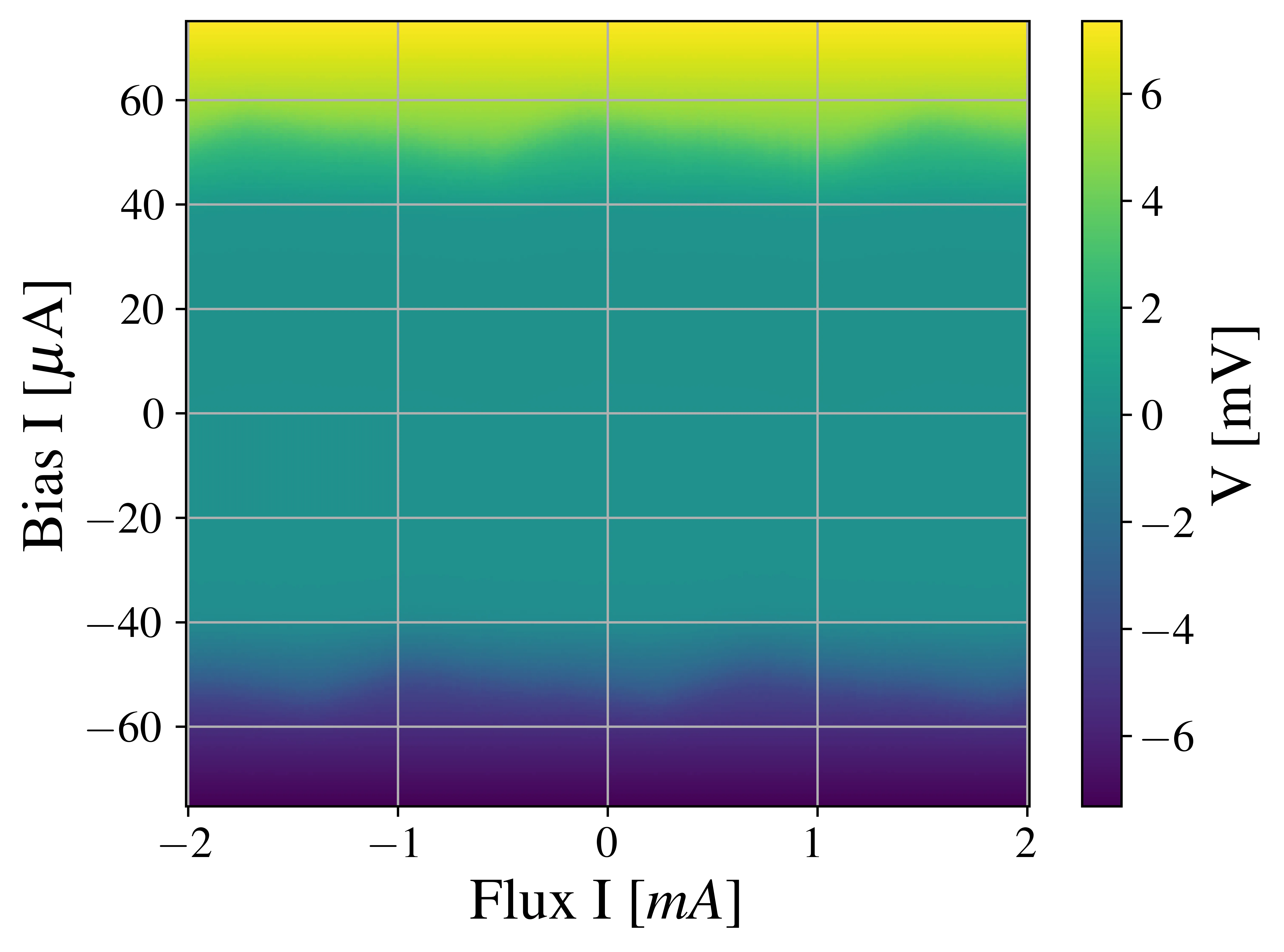
Superconducting circuits often rely on Josephson junctions — places where current flows without resistance through a thin barrier. Typically, this barrier is an oxide layer, but its properties are hard to control at the nanoscale. In this new work, the barrier is a thin layer of niobium or titanium nitride sandwiched between niobium layers.
The researchers fabricated three-dimensional nanobridges using electron-beam lithography and chlorine etching. The top niobium layer provides a high superconducting transition temperature, while the thin nitride layer (NbN or TiN) forms the weak link. This approach allows tuning the superconducting gap and proximity effect without using focused ion beams or oxide barriers.
The devices were integrated into SQUIDs, ultrasensitive magnetic field sensors, and their operation was confirmed at the circuit level. This paves the way for scalable production of oxide-free Josephson junctions for superconducting electronics.
Original abstract
as written by the authors arXiv:2603.20757
We report the realization of multilayer three-dimensional nanobridge Josephson junctions based on Nb/NbN and Nb/TiN superconducting stacks fabricated using electron-beam lithography and chlorine-based dry etching. In this architecture, a high-resistivity nitride layer defines the geometrical weak link, while the top Nb layer sets the overall critical temperature and film quality of the stack. This multilayer design enables engineering of the superconducting gap and proximity effects without relying on focused ion beam milling or oxide tunnel barriers. The devices are successfully integrated into dc SQUIDs, demonstrating reliable circuit-level operation. By combining material selectivity with three-dimensional geometry, this platform provides a scalable route toward oxide-free Josephson junctions suitable for superconducting electronics.
Niobium becomes superconducting at about 9.2 K — higher than liquid helium's temperature, so it can be cooled relatively cheaply.