A siliconsubstrate is a flat, thin slice of crystalline silicon that serves as the foundational layer upon which electronic circuits, optical components, or other thin films are fabricated. It is the starting material for most integrated circuits, microprocessors, and many types of sensors. The substrate's purity, crystal orientation, and surface quality are critical because they influence the performance and yield of the devices built on top.
History
The use of silicon as a semiconductorsubstrate dates back to the 1950s, when it replaced germanium in early transistors due to its superior thermal properties and the ability to grow a stable native oxide (silicon dioxide). The development of planar technology by Jean Hoerni and others at Fairchild Semiconductor in 1959 made silicon substrates the standard for integrated circuits.
How it works
Siliconsubstrates are typically cut from a single crystal ingot grown via the Czochralski process, then polished to a mirror finish. Device layers are added through processes like doping (adding impurities to modify conductivity), deposition (e.g., of oxides or metals), and lithography (patterning). The substrate provides mechanical support and electrical isolation, and its semiconductor properties allow the creation of transistors and other active components.
In practice
Siliconsubstrates are used in virtually all modern electronics, including computer processors, memory chips, solar cells, and MEMS devices, as well as in research on quantum computing and photonics.
Fun fact
A single 300-millimeter silicon wafer can yield over 500 individual processor chips, each containing billions of transistors.
A drop detaches from a faucet nozzle, and a thin filament trails behind it. At the last instant, the filament breaks not in one place but in two—and between them, a tiny sphere, a satellite droplet, hangs suspended. This "debris" of secondary droplets clogs printheads, ruins microchips, and throws off the accuracy of drug dosing.
You can make light turn on command, like water in a hose — if you know where to squeeze. That's what electro-optic circuits do: they change the direction of a beam inside a chip using an electric field. The classic material for such tricks is lithium niobate, a crystal that responds to voltage like a string to a pluck.
A drop of water on glass trembles and shimmers: it seems to have a life of its own. Similar behavior can now be observed in the world of colloids: tiny particles suspended in a liquid. Researchers simulated particles that emit chemical signals. These signals, like scents in the air, spread around and cause neighbors to either draw closer or move apart.
Two transparent sheets with circles drawn on them. If you stack them exactly, the circles align. But give one sheet a slight twist, and a new pattern emerges: in some places the circles bunch together, in others they spread apart. That's roughly how moiré works — an unexpected pattern born from rotating two periodic structures.
Imagine a multilayered shell where metal and insulator layers alternate like pages in a book. Such a structure can make an object hidden inside invisible to an observer. Light bends around it as water smoothly flows around a smooth stone: no ripple, no splash — no reflection, no shadow.
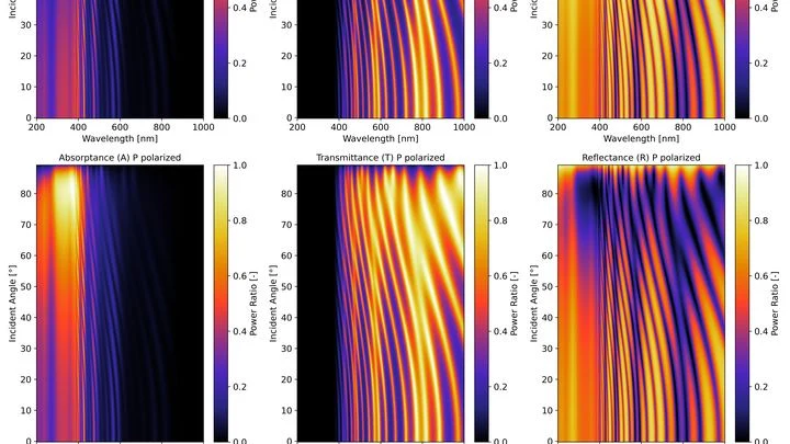
An ordinary sheet of paper looks white because it scatters all light rays chaotically. But a butterfly's wing shimmers blue and green without a drop of paint: its surface is covered with microscopic grooves that dampen some light waves and amplify others. Engineers have long dreamed of replicating this trick: creating a material that colors itself simply by trapping light in the right places.
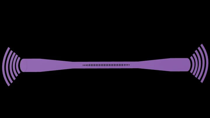
You can launch sound in a crystal at a frequency so high that the human ear can't hear it, and make that sound run in circles, like a train on a loop track. Engineers took a thin film of silicon nitride, deposited it on a lithium niobate substrate, and carved waveguides for sound waves into it.
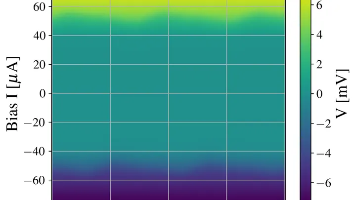
Superconducting circuits often rely on Josephson junctions — places where current flows without resistance through a thin barrier. Typically, this barrier is an oxide layer, but its properties are hard to control at the nanoscale. In this new work, the barrier is a thin layer of niobium or titanium nitride sandwiched between niobium layers.
An ordinary kitchen thermometer shows the temperature at which mercury stops resisting electricity. For superconductors used in quantum computers, the critical temperature is like a quality passport: the higher, the better.
The microchips inside smartphones and computers are getting denser: billions of transistors are packed onto a sliver of silicon the size of a fingernail. When they work, they give off heat like tiny stoves. If that heat isn't drawn away, the chip overheats, starts glitching, or fails outright.
Two-dimensional bismuth on a silicon substrate is a promising material for future electronics. Its edges conduct current without loss, like a highway with no traffic lights. But bismuth itself is delicate: air and moisture quickly degrade its properties.
A quantum computer is like a musical instrument: even a tiny scratch on a string ruins the sound. Instead of strings, we have superconducting resonators — thin traces of titanium nitride on a silicon wafer.
Silicon is like a universal building block: it goes into the chips in your phone, solar panels, and lasers. But if you squeeze it with immense force, the atoms rearrange into new patterns: these forms are called allotropes. One of them, Si-XIII, was first spotted more than twenty years ago, but its exact pattern remained a mystery.
Hydrogen is a clean fuel: when it burns, it produces only water. But to extract it from water, you need to break the strong bond between hydrogen and oxygen. This is usually done with platinum, an expensive metal.
A quantum bit is like a spinning top that must keep spinning steadily for a long time. In germanium, researchers have learned to set such tops spinning, but the floor around them is always trembling: electrical noise knocks the spin off course.
The young star PDS 66 is surrounded by a flat disk of gas and dust — the cradle of future planets. In the cold outer regions of such a disk, silicon and sulfur are usually hidden inside dust grains, but astronomers spotted a bright patch of gas at about 60 astronomical units from the star.
A quantum computer is like an orchestra where every musician must play in perfect harmony. If even one instrument is off-key, the melody falls apart. Superconducting qubits play the role of these musicians, and their "off-key" is the loss of quantum coherence.
An ordinary rubber pad dampens vibration the way a thick blanket muffles sound: the thicker and heavier, the better. Engineers have long dreamed of a material that is light yet "eats" oscillations as well as a massive damper.
A quantum computer is like an orchestra that has to tune its instruments before every piece. Tuning takes time and requires quiet — in our case, deep cold. For silicon chips with boron atoms, this tuning is usually done with microwaves, slowly and only at temperatures below 2 kelvin (minus 271 degrees Celsius).
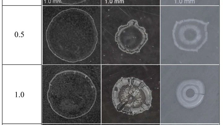
A coffee drop on a table dries and leaves a ring — coffee particles gather at the edge. But if charged nanoparticles float in the drop, the picture becomes richer: the deposit cracks like mud in a dried-up puddle. Physicists studied how the particle charge and the surface on which the drop dries change these cracks.
A silicon wafer is like cookie dough. Heat it in an oven, and tiny raisins appear inside — defects in the crystal lattice that can emit single photons. These "raisins" are called color centers, and they are needed for quantum computers and secure communication.
Light usually tends to scatter in all directions, like splashes from a thrown stone. But it can be caught in an invisible cage where it swirls in place, losing almost no energy. Physicists have built just such a cage using the magnetic material CrSBr — a layered crystal that can be split into flakes just a few atoms thick.
Light passing through a window pane refracts the same in all directions. But in thin layered crystals, it's a different story: light traveling along the layers sees the material differently than light traveling across them. It's as if a sheet of paper were transparent but transmitted light differently along and across its fibers.
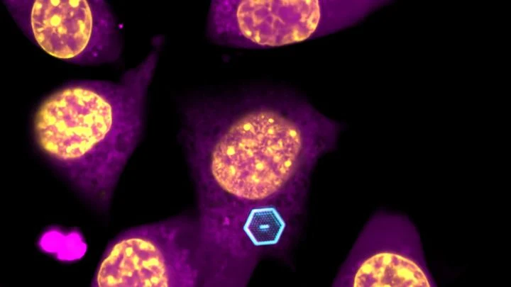
You can trap light in a cage smaller than a speck of dust. Photonic crystals are lattices that stop light from scattering and force it to run in circles. Previously, such structures were grown on a bulky substrate, making them too large for living cells.
Deep inside an underground laboratory, a room-sized detector waits for an event that might happen once in a hundred million billion years. That event is neutrinoless double beta decay — a process that would break one of physics' fundamental laws. To catch it, you need perfect silence: not a single stray radioactive atom in the detector's materials.
A quantum computer is like an orchestra that can only perform in complete silence. The slightest noise, and the delicate melody falls apart. For quantum devices, heat is that noise: even faint infrared radiation from nearby components heats up the qubits and erases their quantum states.
A laser beam usually looks like a straight column of light. But if you pass it through a wafer with a pattern thinner than a hair, the beam scatters into thousands of tiny pockets of light. In each pocket, you can suspend a single atom, like a pea in a dimple.
Two pieces of graphite rub against each other, and the resistance vanishes as if an invisible film of oil separated them. Previously, this was only seen under a microscope, on tiny contact patches.
A fusion reactor resembles a giant boiler where hydrogen is 'cooked' into helium. The plasma inside is heated to 150 million degrees — ten times hotter than the Sun's core. But like any boiler, scale forms: harmful impurities that settle on the walls and quench the plasma.