Artificial atoms gain new orbitals express
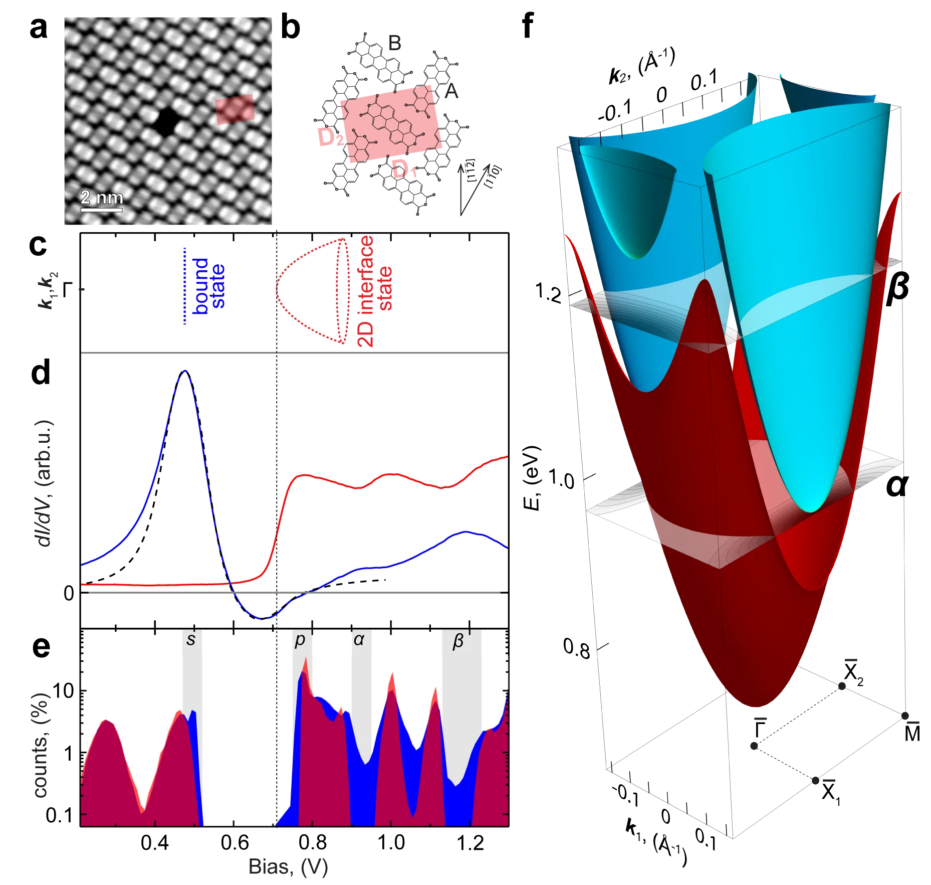
A wafer-thin film of organic molecules was grown on a silicon substrate. In this film, as if on a sheet of graph paper, tiny "pens"—artificial atoms — were laid out with the tip of a scanning tunneling microscope. Electrons inside such a pen behave like electrons in a real atom: they occupy specific energy levels that resemble the familiar s- and p-orbitals. These levels even allow neighboring pens to "bond" with each other, like atoms in a molecule.
But the most interesting part begins when an electron tries to escape the pen. The surrounding film is arranged so that in some directions the electron has a clear path, while in others it is completely blocked. New orbitals emerge, stretched along the allowed directions like long corridors. Real atoms do not have such orbitals. They resemble wires laid out in a two-dimensional world.
The discovery expands the vocabulary of chemistry: now, when designing materials, we can use not only the familiar s-, p-, and d-orbitals but also new ones born from the two-dimensional vacuum. Perhaps in the future this will lead to electronics where current flows along pre-drawn lines without any wires.
A scanning tunneling microscope does not "see" atoms in the usual sense: it probes the surface with a needle whose tip is thinner than a single atom, and builds a map from the current flowing between the needle and the sample.