Layered crystal boosts light sevenfold express
An ordinary piece of semiconductor weakly changes the color of light passing through it. For decades, physicists worked around this limitation by placing the crystal in clever surroundings, but the material itself remained the same.
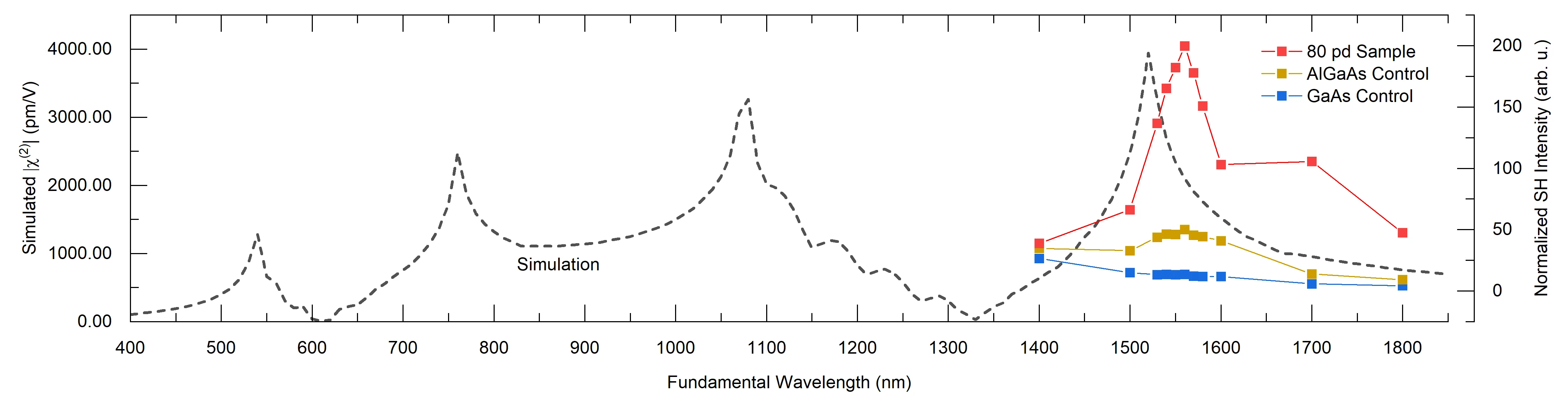
Now researchers have assembled a "sandwich" of alternating thin layers of gallium arsenide and aluminum gallium arsenide. When light enters such a layered crystal, it makes electrons jump between layers, and in response, a wave with doubled frequency is born. An infrared beam with a wavelength of 1550 nanometers turns into green light with a wavelength of 775 nanometers.
To make the layers perfectly flat, the scientists paused during crystal growth. Electron microscopy showed that the boundaries between layers became sharper, and efficiency increased. Calculations promise even more — up to 7 nanometers per volt for more complex structures.
Such a material could be useful in quantum communication: it can generate pairs of entangled photons at telecommunications wavelengths — exactly what is needed for secure data transmission.
Original abstract
as written by the authors arXiv:2602.23246
The recent, rapid advances in nonlinear chipscale nanophotonics in the visible and near-infrared have been largely driven by manipulating the local dielectric environment proximate to decades-old workhorse bulk nonlinear optical materials, rather than increasing the inherent strength of their nonlinear response. While proposed decades ago, we demonstrate the first experimental realization of a new class of designer nonlinear materials that leverage the interband optical transition in asymmetric structures to provide strong second order susceptibility, $$\chi^{(2)}$$. Using simple AlGaAs/GaAs coupled quantum wells operating in the near-infrared as a prototype, we observed strong second harmonic generation enhancement of 1550 nm to 775 nm over bulk controls. Extracted $$\chi^{(2)}$$ values were as high as 2750 pm/V, which is $$>$$7x that of bulk GaAs. Furthermore, measured susceptibilities agreed well with quantum mechanical calculations of $$\chi^{(2)}$$ using layer profiles extracted from electron microscopy. Growth interruptions were employed to improve interfacial abruptness in response to electron microscopy characterization, resulting in increased $$\chi^{(2)}$$ toward the simulation predictions for ideal heterointerfaces. More complex layer designs showed predicted $$\chi^{(2)}$$ up to 7 nm/V. Such materials are anticipated to find myriad applications, including entangled photon generation at telecommunications wavelengths for chipscale quantum information processing.
The transition from infrared to green light is a frequency doubling. If sound doubled its frequency the same way, the note C would become the C of the next octave.
In the series "Star Trek," quantum entanglement is used for instantaneous communication; the layered crystals from this work could become a source of entangled photons for such a network.