Electron microscopy is a family of techniques that use a beam of electrons to image objects at resolutions far beyond the limit of optical microscopes. Because electrons have a much shorter wavelength than visible light, they can resolve details down to the atomic scale. This has revolutionized biology, materials science, and nanotechnology by allowing direct visualization of viruses, molecules, and crystal defects.
History
The first electron microscope was built by Ernst Ruska and Max Knoll in 1931, for which Ruska received the Nobel Prize in Physics in 1986.
How it works
A beam of electrons is focused by electromagnetic lenses onto a thin specimen. The electrons interact with the sample, being scattered or absorbed, and the resulting pattern is magnified and projected onto a detector to form an image. In scanning electron microscopy (SEM), the beam is rastered across the surface, and secondary electrons are collected to build a topographical image. In transmission electron microscopy (TEM), electrons pass through the sample, revealing internal structure.
In practice
Used extensively in materials science to characterize nanostructures, in biology to image cellular organelles, and in the semiconductor industry for quality control of microchips.
Fun fact
The resolution of a modern electron microscope is so high that it can image individual atoms, making it possible to see the positions of atoms in a crystal lattice.
On the table lies a layered cake of hexagonal boron nitride flakes, a material similar to graphite but made of boron and nitrogen atoms. One flake is carefully transferred onto another, and at the spot where they overlap, after heating in oxygen, bright single light sources are born.
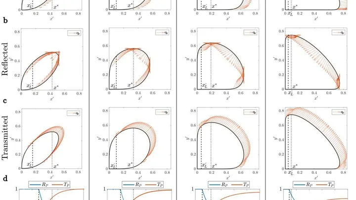
Light knocks electrons out of a crystal, and they fly toward the detector like arrows toward a target. From their trajectories, physicists reconstruct how electrons behaved inside the material: with what energy and in which direction they moved. But switch on a magnetic field, and the trajectories bend. The arrows start to curve, the target turns into a warped mirror, and the picture blurs.
The electron beam of a microscope usually flies through emptiness, like a courier on an empty highway. Any air molecule is a bump that makes it bounce and lose direction. So before, to examine a sample, you had to freeze it, dry it, or coat it with metal—and still you could only look in a vacuum.
An electron microscope is a giant pipe organ: instead of pipes (electromagnetic lenses, instead of air) a stream of accelerated electrons. It once merely painted mute frescoes of the atomic world, condemning scientists to grueling decipherment.
A detector filled with superfluid helium-4 is like a perfectly still lake. The liquid doesn't slosh or bubble: it's frozen in a single quantum state. An invisible guest, a dark matter particle, flies through it. It doesn't shine or leave a track. But sometimes it nudges a helium nucleus.
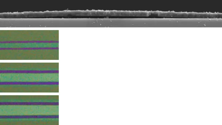
On the surface of a thin film of bismuth iron oxide, you can see neat stripes, like furrows in a plowed field. What lies beneath them has remained a mystery until now.
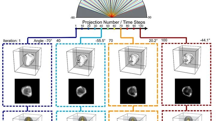
A tiny gold star melts under the beam of an electron microscope, its points slowly rounding off. In the past, such a process could only be seen in snapshots taken with long pauses, and the probing beam itself would alter the sample.
An ordinary sheet of paper looks white because it scatters all light rays chaotically. But a butterfly's wing shimmers blue and green without a drop of paint: its surface is covered with microscopic grooves that dampen some light waves and amplify others. Engineers have long dreamed of replicating this trick: creating a material that colors itself simply by trapping light in the right places.
Tuning a radio to your favorite station is a search for the right frequency amid the noise. The new device does the same, but for waves about three millimeters long. Such waves come from distant galaxies and possibly from dark matter particles. The device is a pattern of superconducting niobium traces on a silicon wafer.
A typical accelerator is like an assembly line where electrons are the workpieces. To get the desired X-ray pulse, the workpiece is fine-tuned after it's already on the line: squeezed, filtered, corrected. In the new work, engineers decided to take a different approach — shaping the workpiece before it even hits the conveyor.
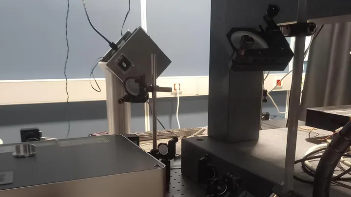
At LCLS-II, electrons are knocked out of a metal by a short laser pulse.
A river flows in one direction, but a wave on its surface travels in the opposite direction. The same splitting happens in hyperbolic materials: the energy of a light wave and its fronts diverge, preventing a sharp lens from being created.
Radio waves that oscillate less than once per second pass through the earth and water with almost no loss. Such signals are used to communicate with submarines and to search for minerals. But a conventional antenna for them would need to be hundreds of meters long, and its sensitivity leaves much to be desired.
In a piece of manganese oxide just a few atomic layers thick, electrons behave like a crowd on an escalator: each moves by its own rules, but together they create a common flow. Physicists shone soft X-rays on such a film and knocked electrons out.
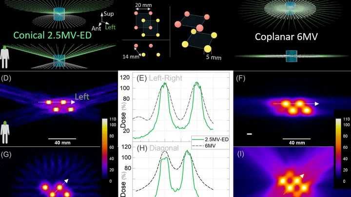
Radiation therapy is like shooting at a small target with a very large-caliber rifle: even a precise shot hits a large area around it. The thickness of the 'trace'—called the penumbra — is 2–3 millimeters in standard machines. For a tumor in the lung, that's not a big deal, but next to a nerve or a blood vessel, those millimeters decide whether a person stays healthy.
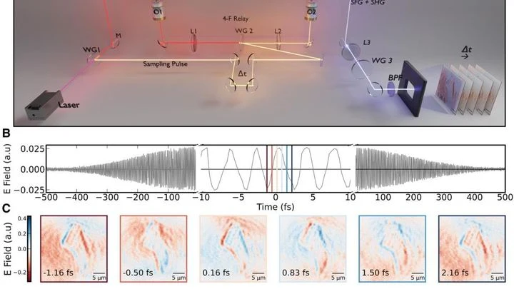
Light is not just a beam but a wave with an electric field that changes at a speed unimaginable to ordinary clocks. Until now, this field could only be measured at a single point, like taking temperature with a single thermometer. Now researchers have created a method that shows the entire field at once, like a thermal imager showing a heat map.
An X-ray image of a battery looks like a photo taken through frosted glass: fine details blur into a gray smudge. The culprit is the detector itself, which cannot distinguish features smaller than its pixel size. Engineers proposed getting around this barrier by illuminating the sample not with a uniform beam but with a striped pattern.
An electron beam can be compared to the light from a laser pointer: if it diverges, the spot on the wall quickly spreads out. In the lab, physicists created such a narrow beam that it remained thin over a long distance, like the beam of a good pointer.
A laser beam passes through glass and touches a thin diamond film. At the point of contact, the film turns into a narrow strip that lifts slightly. We place a second strip next to it, and between them remains an empty corridor. That's the channel: its width can be fifty times its height, like a sheet of paper lying on a table.
A heart cell in a Petri dish contracts, and at that moment, an electrical wave sweeps across its surface. Previously, to catch that wave, you had to poke the cell with an ultra-fine electrode needle. Now, you just look at it under a microscope.
The method is called electrochromic recording.
You can't catch X-rays from stars with an ordinary mirror: they pass through glass like light through a window pane. To reflect them, you need a mirror almost parallel to the beam: then the X-rays skim along the surface like a flat stone skipping on water, only slightly changing direction.
A typical 3D printer squeezes out plastic like a pastry chef piping cream from a bag. Here, instead of plastic, it's light. A laser beam draws in liquid resin, making it solidify at precise points. This creates parts too small to see without a microscope.
Until now, such printers were slow: the beam crawled across the surface like a pen on paper.
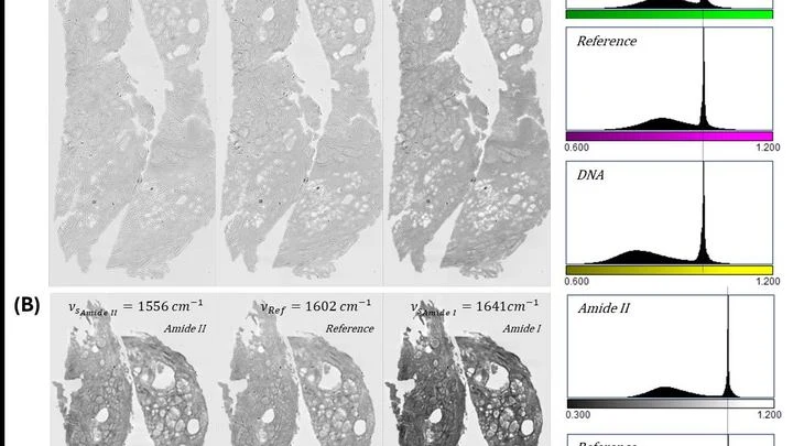
A pathologist looks through the eyepiece and sees a pink-purple tissue section — the classic hematoxylin and eosin stain. The dyes bind to nuclei and cytoplasm, and the color tells the doctor about the disease. But preparing the slide itself takes hours: fixation, paraffin embedding, sectioning, staining.
This new device skips the dye.
A printer that prints not with ink but with metal and ceramic is now a reality. Scientists took an ordinary drop of water containing dissolved metal salts and made it deposit copper, zinc oxide, or nickel hydroxide onto a surface — all with precision down to millionths of a meter.
The secret lies in electricity.
A camera that sees ultraviolet light typically costs as much as a nice car. That's because it requires a special crystal and a complex fabrication facility. Engineers in Korea took a different approach: they grabbed a run-of-the-mill chip, the kind made by the millions for phones, and sprayed a thin layer of metal-oxide nanoparticles onto it, like paint from a can.
A thin film of thorium dioxide, just 10 nanometers thick, is deposited on a steel disk. A laser pulse strikes it, but instead of the expected glow, the detector catches a stream of electrons.