Quantum Pairs: How Defects in a Crystal Change the Game express
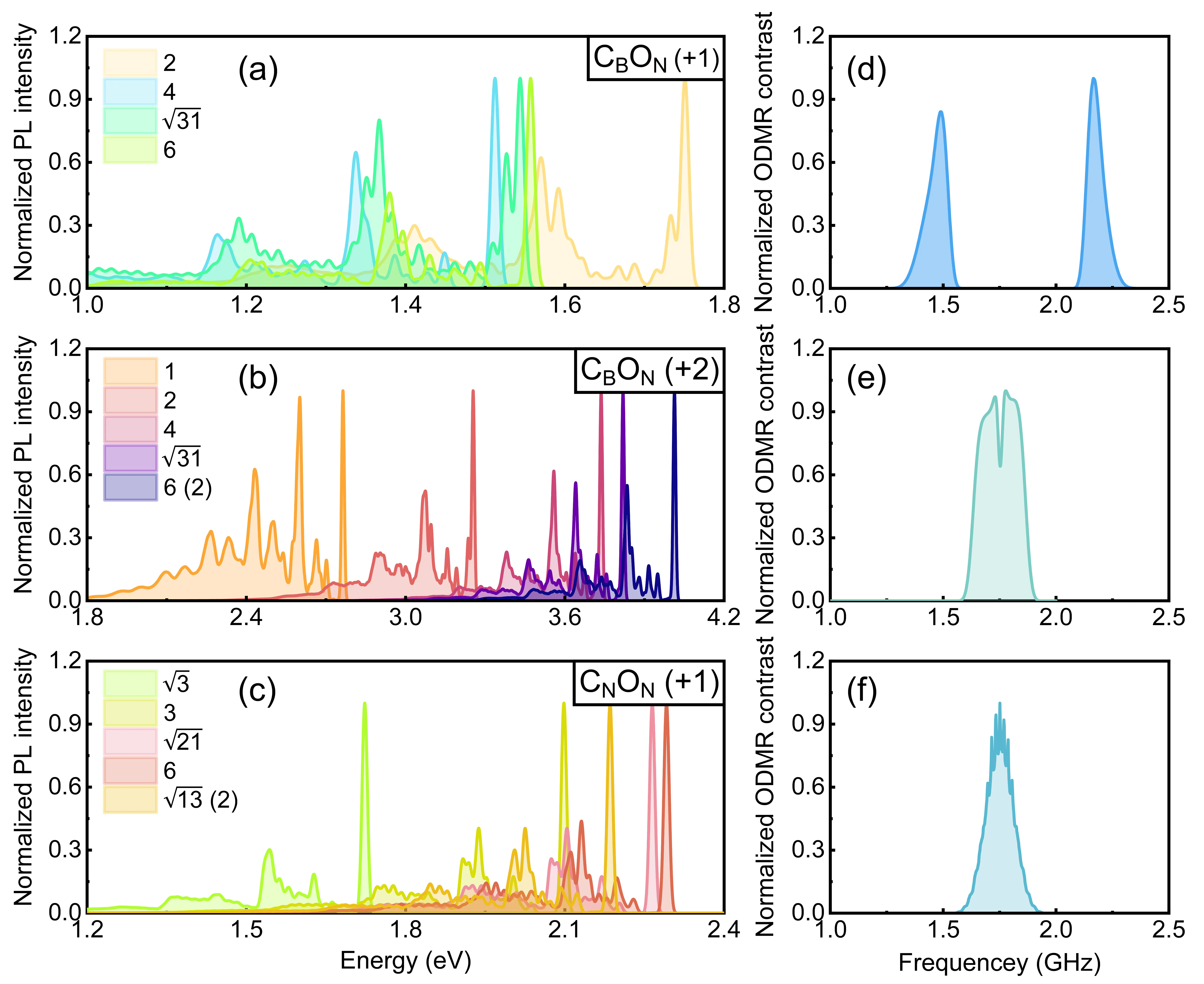
In a boron nitride crystal, the perfect atomic lattice is sometimes disrupted: an atom is missing here, or replaced by a foreign one there. Under a powerful microscope, these tiny imperfections appear as traps for electrons: they capture particles and start to emit light, and they also respond to magnetic fields. It is precisely such defects that promise to become the foundation for quantum technologies operating at ordinary room temperature, without bulky refrigerators.
For a long time, it was believed that each defect was a loner. But supercomputer calculations revealed a different picture: defects often live in pairs, like two communicating vessels. One of them is a donor with an extra electron, the other is an acceptor that lacks an electron. The electron jumps from the donor to the acceptor, and the distance between them determines everything: the color of the emitted light, its brightness, and how long it lasts. By changing this distance, one can tune the quantum properties of the pair, as if turning a tuning knob.
When there are many such pairs in the crystal, they begin to influence each other, creating entire ensembles. This explains why different laboratories obtained such contradictory results: researchers were seeing the emission not of individual defects but of entire collectives, where each pair contributed its share. Now, with this knowledge, one can not guess but precisely design the desired configurations of defects — for example, to obtain a perfectly stable source of single photons for quantum communication.
Original abstract
as written by the authors arXiv:2605.20655
Optically addressable spin defects in hexagonal boron nitride hold promise for room-temperature quantum technologies, but their microscopic identities remain largely unknown. Using first principles calculations, we show that coupled spin optical signals arise from interacting donor acceptor pairs, not the commonly believed isolated defects. Intra and inter pair separations control charge transfer, electronic structure, and spin coupling, thereby greatly modulating zero phonon lines, phonon sidebands, lifetimes, and the sign of optically detected magnetic resonance contrast. Importantly, we identify two distinct charge-state-dependent coupling regimes and extend this picture to correlated defect ensembles, explaining the wide diversity of experimental observations. Our results establish a microscopic framework for coupled defect behavior and provide design principles for spin-active quantum emitters in wide bandgap semiconductors.
Boron nitride is sometimes called 'white graphene' due to its similar layered structure, but unlike graphene, it does not conduct electricity, making it an ideal platform for isolating quantum defects.