Light from an Atomic Gap express
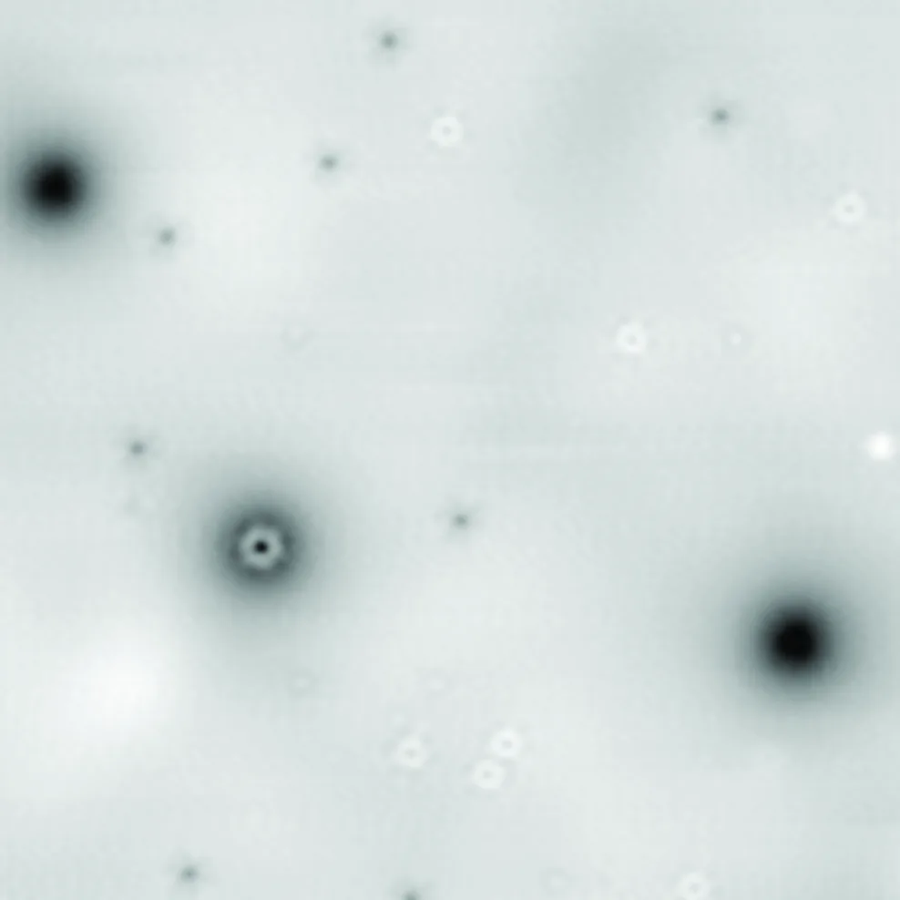
The tip of a scanning tunneling microscope approaches a crystal surface so closely that an electric current jumps between them. Electrons from the needle are injected into a layered semiconductor and land in an atomic vacancy — a spot where one atom is missing from the lattice. This void acts as a tiny trap for charge.
When an electron and a hole meet in such a trap, a single photon is born. The light escapes and can be caught by a detector. The emission pattern mirrors the shape of the vacancy's electron cloud, like a fingerprint that reveals exactly which defect we are dealing with. The method's resolution is below one nanometer, thinner than a chain of ten atoms.
This experiment links electrical control with optical readout at the scale of a single atom. Such an interface is needed for quantum computers and secure communication lines, where information is carried by single particles of light. Instead of bulky lenses and lasers, an ultra-fine needle and an electrical pulse.
The current through the microscope tip is so tiny that in one second it carries roughly as many electrons as grains of sand that fit in a thimble.