A Lens the Size of a Nanoparticle
Light passing by a tiny structure changes direction. If the structure is smaller than the wavelength of the light, it acts like a lens and focuses the light into a spot smaller than the wave itself.
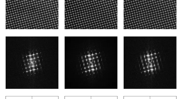
The ability of an imaging technique to resolve features at the scale of individual atoms.Atomic resolution refers to the ability of an imaging technique to distinguish individual atoms, typically at a scale of less than one nanometer. This capability is crucial for understanding the structure and behavior of materials at the most fundamental level, enabling scientists to see the exact arrangement of atoms in crystals, surfaces, and even single molecules.
The first atomic-resolution images were obtained in 1981 by Gerd Binnig and Heinrich Rohrer with the invention of the scanning tunneling microscope, for which they won the Nobel Prize in Physics in 1986.
Atomic resolution is achieved through techniques like scanning tunneling microscopy (STM) and atomic force microscopy (AFM), which use a sharp tip to probe the surface atom by atom. Alternatively, aberration-corrected transmission electron microscopy (TEM) can focus electrons to a point small enough to resolve individual atomic columns. These methods rely on quantum effects, such as electron tunneling or atomic forces, to map the positions of atoms with extreme precision.
Atomic resolution imaging is used in semiconductor manufacturing to inspect chip features, in catalysis research to observe active sites, and in materials science to design new alloys and nanomaterials.
With atomic resolution, scientists have captured images of individual atoms moving across a surface, directly observing diffusion processes in real time.