An Ion Beam Scalpel for Superconducting Circuits express
A potter uses a sharp stylus to trace a pattern on a still-damp clay tile. One wrong move, and the line blurs, the tile cracks. Physicists work with films of the high-temperature superconductor YBCO (a compound of yttrium, barium, copper, and oxygen) in much the same way. Only their stylus is an ultra-fine beam of helium ions, and the tile is a ceramic layer a few hundred atoms thick.
The authors of the new study watched what happens to such a film when it is bombarded for a long time with helium ions at 30,000 electronvolts. They measured electrical resistance and took X-ray and Raman spectra. It turned out that at low doses, point defects appear in the crystal — oxygen atoms are knocked off their sites but don't leave the material; instead, they get stuck in nearby voids. Such a defect is called a Frenkel pair. The number of charge carriers barely changes, but their mobility drops — electrons more often bump into disorder.
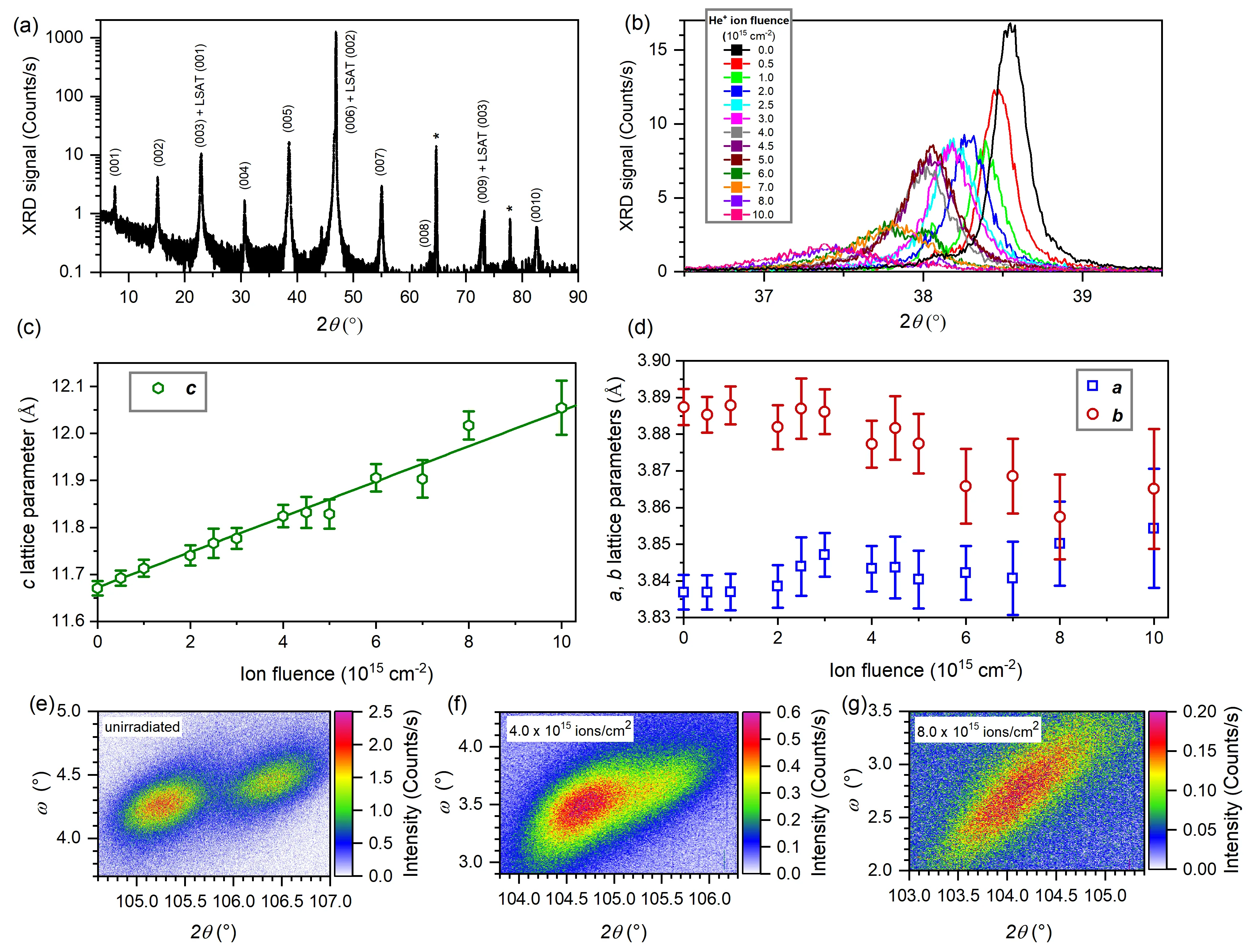
As the dose increases further, the crystal lattice loses its order: X-rays show the layers spreading apart, the unit cell going from rectangular to square, and at 10¹⁶ ions per square centimeter the film turns into amorphous glass. Electrical resistance in the normal state rises sharply, while the critical temperature falls according to a law derived half a century ago by Abrikosov and Gor'kov for the destruction of Cooper pairs by magnetic impurities. Interestingly, the anisotropy, the difference in properties along and across the layers, decreases here, whereas with simple oxygen deficiency it increases. So the beam doesn't just knock out oxygen; it creates a more complex kind of disorder.
This work isn't just physics for physics' sake. It gives engineers precise numbers: how much irradiation is needed to suppress superconductivity in the right places and create a quantum circuit without destroying the substrate. Without that knowledge, the stylus remains blind and the pattern unreliable.
Original abstract
as written by the authors arXiv:2606.14588
Focused helium ion beam (He-FIB) irradiation with 30 keV ions is a key tool for nanoscale patterning and defect engineering in high transition temperature (Tc) cuprate superconducting devices, yet its usable fluence window is constrained by the competing requirements of reliable superconductivity suppression and minimal structural degradation. In this work, we provide a comprehensive dataset on the effects of large-area 30 keV He+ ion exposure on the electric transport and superconducting properties of epitaxial YBa2Cu3O7 (YBCO) thin films. X-ray diffraction shows a fluence-driven loss of crystalline order accompanied by an out-of-plane lattice expansion and an orthorhombic-to-tetragonal transition, culminating at predominant amorphization at the highest fluence of 1 x 10^16 cm^-2. Raman spectra exhibit increasing disorder while lacking signatures of oxygen depletion, indicating that irradiation mainly generates oxygen-related Frenkel defects rather than changing the carrier concentration. Consistently, with increasing fluence, the normal-state resistivity \rho_N(T) at temperature T above Tc increases strongly, while d \rho_N/d T remains nearly unchanged at moderate fluence. The suppression of Tc is accurately described by Abrikosov-Gor'kov pair breaking and reaches complete quenching of superconductivity at 4.5 x 10^15 cm^-2. The anisotropic upper critical fields decrease approximately exponentially with increasing fluence, the vortex activation energy is reduced, and the anisotropy drops, in contrast to oxygen-depleted YBCO. Hall-angle analysis confirms a nearly constant carrier density but a systematic increase in defect scattering and reduced mobility, consistent with a crossover toward the dirty limit at high fluence. These results establish quantitative fluence thresholds and a practical operational window for He-FIB nanopatterning of YBCO quantum circuits.
The helium ion beam is focused to a spot less than ten nanometers in diameter — thousands of times thinner than a human hair.