Where the Electron Lives: Topology of the Band Structure in Real Space ✛
Context
Topological properties of electronic bands are usually studied in momentum space, through Berry phases and symmetry indicators. But the wavefunction from which these properties derive lives in real space, inside the unit cell. Related works in our archive have already shown how STM can reveal topology through defects, boundaries, or interference patterns, for example in graphene-based quantum materials and superconductors. This work follows the same vein but takes a more direct route: it tracks the shift of the charge center within a single band without breaking the crystal's translational symmetry.
Methods
WSe₂ and NbSe₂ samples were grown using self-flux and chemical vapor transport methods, then exfoliated into monolayers on graphite substrates. To precisely register STM images to the atomic lattice, substitutional impurities were introduced: sulfur replacing selenium and molybdenum replacing tungsten, thereby identifying atomic positions. The energy positions of the Γ and K points were determined via constant-current dI/dV spectroscopy, and the spatial charge distribution was measured by varying the bias voltage during scanning, which eliminated drift. In parallel, first-principles calculations with projection onto Wannier functions were performed.
Results
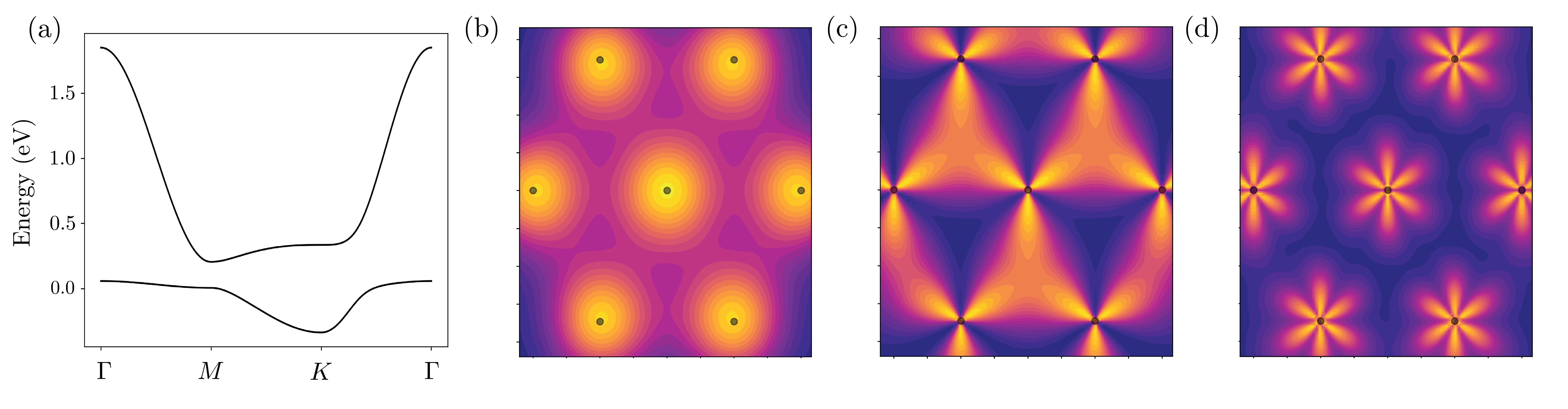
In WSe₂, at a bias of −1.4 V (near the K point), tunneling current maxima appeared at the centers of hexagons, while at −1.9 V (closer to the Γ point), they were on tungsten atoms. The shift amounted to about 0.16 nm, half the distance between neighboring tungsten atoms. In NbSe₂, where the Γ and K pockets overlap in energy, no such shift occurs: charge is always localized on selenium atoms. This agrees with calculations: in WSe₂, the Wannier functions of the valence band are centered in voids, while in NbSe₂, they are centered on atoms. The difference is explained by the fact that in WSe₂, the K point has a chiral d-orbital state with a nontrivial phase upon 120° rotation, which forbids localization on an atom.
Implications
This work demonstrates for the first time that topological obstruction can be diagnosed by a purely real-space signature, the shift of the charge center within a band, without resorting to edge states or defects. This distinguishes it from related studies where topology manifested through boundaries or interference. The method is applicable to any crystal with an isolated band and high-symmetry points separated in energy. For condensed matter physics, this means STM becomes a tool to verify symmetry indicators directly in coordinate space.
Future development
The method can be extended to other obstructed insulators, for example, 1H polytypes of transition metal dichalcogenides, where corner states are predicted. It is also interesting to investigate how the charge shift depends on temperature, strain, or electric fields. In metallic systems such as NbSe₂, topology could be probed through quasiparticle interference near defects, as was done for graphene. Another avenue is combining STM with inelastic tunneling to directly measure Berry phases.
Impact
The result will influence the interpretation of STM images of transition metal dichalcogenides, where bright spots are often mistakenly attributed to chalcogen atoms. This is important for defect inspection and quality control of two-dimensional semiconductors in electronics and optoelectronics.
Next steps
Verify the reproducibility of the charge shift in other obstructed insulators, such as MoS₂ or WS₂. Investigate the influence of spin-orbit coupling on the spatial charge distribution near the K point.
Key open problems
This work directly addresses the problem of classifying topological phases in real space: until now, there was no universal way to distinguish an obstructed atomic insulator from a trivial one without calculating the band structure. The charge shift discovered here could become such an experimental criterion. An open question remains how to generalize the method to bands with strong orbital mixing or to systems with multiple intersecting bands.
The knowledge machine's view
This section is addressed to the author of the paper and their colleagues. Neighbouring works were found by meaning-based search across our archive, not by word overlap. We do not review: we show the field around the work.
What the work does
The study shows that in WSe₂, the maximum of the valence band density of states shifts from tungsten atoms to the centers of hexagons as the energy changes from the Γ to the K point, as captured by STM and consistent with Wannier function calculations. The shift is interpreted as a direct manifestation of topological obstruction in real space, without invoking edge states or defects.
Where its strength is
Direct observation of the charge center shift within a band provides a simple and local signature of topology that can be applied to a broad class of materials with isolated bands.
Where it could go next
- It might be interesting to compare this approach with the analysis of charge zeros, where topology appears at special points of the wavefunction, complementing the picture of Wannier center shifts.based on: How to See Electron Topology in the Zeros of Charge arXiv:2607.21699
- Closely related is the study of fractional charge in twisted materials: there, local charge measurements also reveal topology, and comparing the methods could strengthen the interpretation of STM data.based on: Fractional charge in twisted material arXiv:2602.04561
- One should consider the connection with the work on an insulator edge that conducts like a metal: if there is obstruction in the bulk, edge states should exist, and a combined analysis of bulk and edge could provide a complete picture.based on: The Edge of an Insulator Conducts Electricity Like a Metal arXiv:2605.17335
Worth trying
- Test the method on other transition metal dichalcogenides with known topological invariants to verify the universality of the signature.
- Perform STM measurements at the edges of WSe₂ samples and compare with the charge shift pattern in the bulk to see how the obstruction manifests at the boundary.
- Use substitutional doping to controllably change the energies of the Γ and K points and track how this affects the spatial charge distribution.
Why this may matter
Such an approach could turn STM into a standard tool for probing topological invariants in coordinate space, which is especially valuable for materials where momentum space is difficult to access.
Nearby works in our archive
- How to See Electron Topology in the Zeros of Chargesimilarity 0.56
- Hidden states on the surface of a uranium superconductorsimilarity 0.54
- Fractional charge in twisted materialsimilarity 0.53
- Lone Electrons and Pairs with a Twist: A New Look at Superconductorssimilarity 0.53
- The Edge of an Insulator Conducts Electricity Like a Metalsimilarity 0.52
- Invisible Superconductivity in Twisted Layerssimilarity 0.51
The archive is sparse around this work: the closest review is only 0.56, against a usual 0.64. It looks like few have drilled nearby.
The distance over which the charge maximum shifts in WSe₂ is only 0.16 nanometers, roughly 600 times smaller than the thickness of a human hair.
In Greg Egan's novel 'Permutation City', characters manipulate quantum states to alter the properties of matter. Here, scientists are essentially taking the first step toward such control: seeing where exactly in the crystal the electron lives and how that relates to global topology.
Key numbers
- energy of K point in WSe₂: -1.24 eV
- energy of Γ point in WSe₂: -1.89 eV
- charge shift: 0.16 nm
- energy difference between Γ and K in WSe₂: 0.65 eV
- measurement temperature: 300 K