Tungsten diselenide is a layered compound of tungsten and selenium, belonging to the family of transition metal dichalcogenides. It has a unique electronic structure that changes dramatically when thinned to a single layer, transitioning from an indirect to a direct bandgap semiconductor. This property makes it highly interesting for optoelectronics and valleytronics, where the electron's momentum and spin can be used to carry information.
History
Tungsten diselenide was first synthesized in the 1960s, but its monolayer properties were only explored after the discovery of graphene in 2004. The direct bandgap in monolayers was demonstrated in 2010.
How it works
In its bulk form, tungsten diselenide has an indirect bandgap, meaning electrons need to change momentum to emit light. When exfoliated to a monolayer, the bandgap becomes direct, allowing efficient light emission and absorption. The material also exhibits strong spin-orbit coupling, which couples the electron's spin to its momentum, creating unique 'valley' states that can be selectively excited with circularly polarized light. This allows for control of electronic properties via optical means.
In practice
Used in ultra-thin photodetectors, light-emitting diodes, and valleytronic devices, as well as in studies of exciton physics and quantum optics.
Fun fact
In monolayertungsten diselenide, shining circularly polarized light can create a 'valley polarization' where electrons in different valleys have opposite spins, a property that could be used for future 'valleytronic' computers.
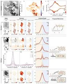
A stack of pages that has been flipped through many times remembers it: some sheets lie flat, others stick up, and creases remain here and there. Layered materials behave much the same way when ions enter them.
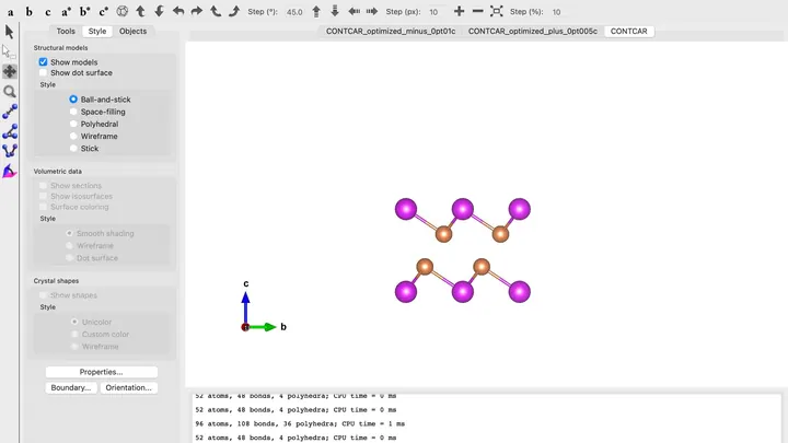
A door lock with two different keys: one turns easily, the other demands noticeable effort. That is how two layers of hexagonal boron nitride behave when twisted relative to each other. This material consists of boron and nitrogen atoms arranged in a hexagonal lattice, and its layers can sit in different registries, like two identical grids shifted by different angles.
A stack of playing cards lies still. You can slide the top card with your finger: that's crude intervention. Or you can blow so that the whole stack momentarily changes shape, but the cards don't scatter. That's roughly how light, in a new experiment, rearranges a crystal of tin selenide (SnSe).
Usually, to change the structure of a solid, you heat it or pass a current through it.
In a two-dimensional crystal of tungsten diselenide (WSe₂), light creates pairs — an electron and a hole that stick together. Such pairs are called excitons. Among them are "dark" ones: they barely emit, but they set the tone at low temperatures.
Hidden within thin layers of tantalum selenide (TaSe₂) is a property that defies conventional physics. When guest atoms were added between the layers of this material, the structure lost its center of symmetry, and inside, superconductivity with armor emerged.
A tuning fork struck once rings pure and long. But if you shake the fork itself while it sounds, the tone wavers and dies out quickly. Something similar happens to electrons in any piece of matter. Atoms in a lattice never stay put: thermal vibrations keep them jittering.
The book is open to the middle. Current runs along the spine, while the pages remain cool. That's roughly how a two-dimensional topological insulator works — a material where electricity flows only along the edges, while the interior stays still.
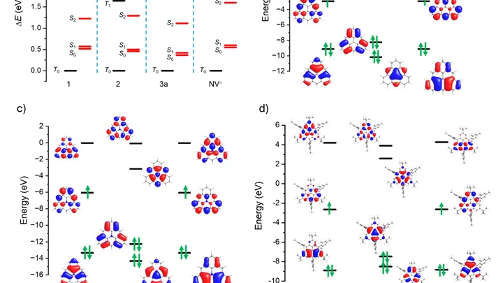
At the heart of a future quantum computer might lie a tiny organic molecule shaped like a triangle. It has two 'extra' electrons that don't pair up. Such molecules are called diradicals, and their electrons can store information in a special, quantum way.
A thin film of molybdenum disulfide, less than a micron thick, acts as a miniature photon-pair factory built right into a fiber-optic connector.
Ordinary optical fiber is not just a glass thread for the internet.
The magnetic field increases, but the magnetization stays put. It's like a scale where you add weight, yet the needle doesn't move until enough has accumulated to jump to the next mark. That's exactly how rare-earth tetraboride crystals behave, and physicists have been puzzled for decades.
A chef pours hot sugar syrup onto a cold table, and it sets into crystals. That's roughly how engineers pictured metal solidification: the liquid instantly becomes a scatter of crystalline grains. But close-up imaging revealed an extra stage wedged between liquid and solid.
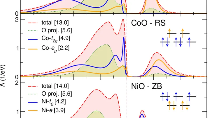
If you change not the composition but only the arrangement of atoms, you can make the same material conduct electricity or absorb light differently. That's exactly what the authors did with nickel and cobalt oxides. In one case, atoms are stacked like balls in a cubic box: each metal atom is surrounded by six oxygen atoms (rock salt structure).
A layered cake of atomic planes of nickel and oxygen: that's how bilayer nickelates are built. Two such planes are separated by a spacer layer. If an oxygen atom sits in that spacer, it acts as a bridge: it links the layers and triggers a state in which electrons move without resistance.
A crystal is like a city: if the streets are crooked, traffic jams. In a crystal, the streets are atomic rows, and the traffic is the flow of electrons. Any tiny imperfection, impurity, or atomic displacement makes electrons scatter. Scientists from several labs have learned to grow crystals so that the "streets" are almost perfectly straight.
The method is called horizontal vapor transport.
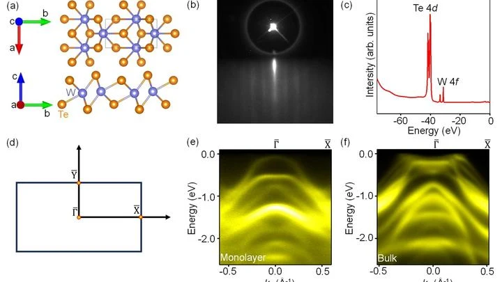
A single-atom-thick sheet of tungsten telluride is like thin foil: electrons can't pass through because there's a band gap between their possible states, like a moat you can't jump across. Add two more layers, and the moat disappears; the material becomes a metal, and current flows. Add more layers, and the properties change again, as if someone is flipping modes with a single button.
A light bulb that shines not in a steady stream but in individual drops — photons. Such 'droplet' sources are called single-photon emitters. They are needed for quantum communication, where each photon carries a bit of information, and for ultra-precise measurements.
A sheet of paper weighs almost nothing, but stack a hundred sheets and you get a noticeable pile. That's roughly what scientists did with a material that excels at converting one color of light into another, but only when it's just one atom thick. A single layer is like a single sheet: it works beautifully, but it's too thin to produce much light.
Rubbing a comb against wool creates a spark. A similar principle works in triboelectric nanogenerators — devices that convert mechanical touches into electricity. The problem is that ordinary materials produce a weak charge.
A thin film of soap on your hand conforms to the shape of your palm, but clench your fingers and the tension changes unevenly. A monolayer of molybdenum disulfide on a graphite substrate behaves in a similar way.
Two sheets of graphene — carbon film one atom thick — without a twist resemble a harbor clogged with shoals: lithium ions either run aground or rush past without stopping. But a 9.43° twist lays out a perfect fairway. The ion ships dock securely to carbon 'piers' and immediately cast off without losing speed.
An alloy of palladium and tellurium with a small amount of gold added behaves like a wire that loses its resistance when cooled. At ambient pressure, the three samples with different gold contents had superconducting transition temperatures of 2.7, 4.1, and 4.6 kelvin — colder than a freezer, roughly like deep space.
A rug lies flat, but if you push it from the edge, wrinkles run across it. In a thin film of tantalum sulfide (1T-TaS2), wrinkles made of electrons, charge waves, freeze as if the rug were stuck to the floor. To move them, you need to apply force. Scientists have found a way to control this force using an electric field and a magnet.
A laser beam twisted into a spiral looks like a drain vortex in a sink: light moves not only forward but also in circles. Such vortex beams already help move tiny particles and transmit more data. But once they pass through an inhomogeneous medium, the vortex falls apart, like water from a leaky bucket.
A sheet of graphene one atom thick is like a flexible metal mesh through which electrons zip almost unimpeded. Stack two such sheets with a slight twist, and the material's properties change dramatically: it can become an insulator that blocks current.
A sheet of graphene one atom thick is like a perfectly smooth tablecloth on which electron marbles roll. Place an electric barrier in their path, and usually they'll bounce back. But in graphene, it's different: under certain conditions, electrons pass through the barrier without even noticing it, as if the wall were made of mist.
The surface of the uranium compound UTe2 crystal looks like a frozen sea: in some places, electrons move freely; in others, they get stuck near atoms. A scanning tunneling microscope, a device that probes the surface with an atomically sharp tip and senses individual electrons, revealed that this landscape is not random.
In a metal crystal, atoms line up in neat rows like bricks in a wall. Knock out a single brick, and you're left with a void — what scientists call a vacancy. Under irradiation, these voids multiply and start merging into large holes, sapping the metal's strength. It's like holes in a brick wall joining up into a gaping breach.
Turning light gases like hydrogen and nitrogen into metal is a long-standing dream of physicists. In a new experiment, nitrogen was compressed to 130–140 gigapascals (pressure equivalent to 14 million kilograms pressing on a fingernail) and heated to 3000°C.
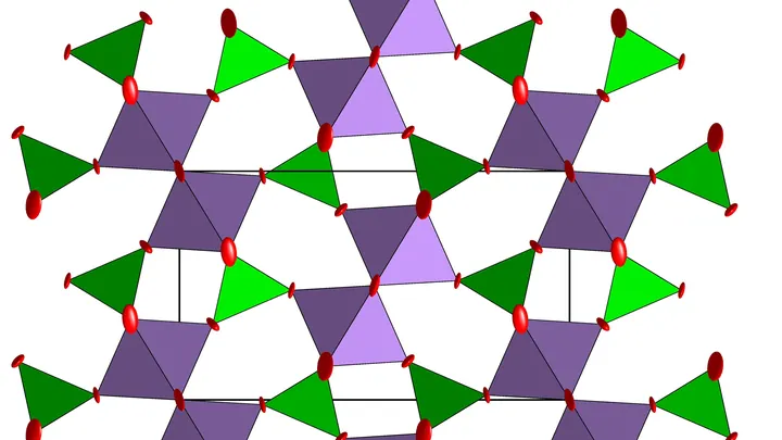
Silicon is like a universal building block: it goes into the chips in your phone, solar panels, and lasers. But if you squeeze it with immense force, the atoms rearrange into new patterns: these forms are called allotropes. One of them, Si-XIII, was first spotted more than twenty years ago, but its exact pattern remained a mystery.
The layered material (SnS)1.15(TaS2) resembles a stack of paper, where the sheets conduct electricity and the interlayers prevent them from sticking together. At ambient pressure, this material conducts current without resistance, making it a superconductor.
A laser flash hits a one-atom-thick layer of silver sitting on bilayer graphene, and within quadrillionths of a second, a gap opens in graphene's electronic structure where none existed before. It's as if an ordinary wire momentarily became a semiconductor: electrons stop flowing freely, and a band gap appears.
Heat dissipates poorly in thin layered materials, like a crowd in a narrow corridor. In ReS2 crystals, layers lie on top of each other, and heat can travel across them. Scientists measured how quickly this happens and found a surprise: when the layers are stacked directly one above the other, heat passes almost twice as fast as when they are shifted.
Twisted layers of atoms in a material form a pattern of tiny regions, domains, each of which can be electrified in one of two directions, like a compass needle pointing north or south. Previously, such materials were studied only as a whole, measuring thousands of domains at once, and their collective behavior was like a choir where individual voices are not heard.
The popping lid of a jam jar is the hero of this story. Press it, and with a loud click it flips from a convex to a concave shape. Exactly the same happens with a hinged beam inside each cell of a new mechanical lattice.
Scientists assembled these snapping beams into a hexagonal grid, like honeycomb, but made of elastic plates. When one beam is sharply compressed, it snaps and pushes its neighbor.
A blunt cylinder flying at six times the speed of sound isn't the most elegant object, but it's the star of a new simulation. The surface of such a vehicle is never perfectly smooth: during atmospheric entry, the heat shield ablates, leaving bumps and pits.
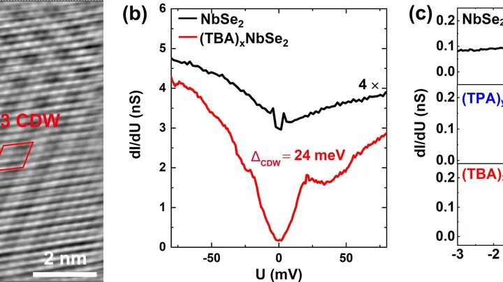
The NbSe2 crystal is like a stack of paper: layers lie tightly packed, and their properties blend together. Chemists found a way to pry this stack apart by nearly double — inserting long organic molecules between the layers like spacers. Now each layer behaves as if it were all alone, just one atom thick.
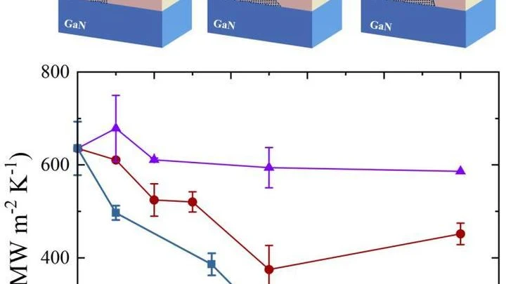
Inside a high-power transistor, heat escapes through junctions between different crystals, like water through narrow locks. For aluminum and gallium nitrides, key materials in power electronics, that lock is often a thin layer of their alloy. It is added deliberately or forms on its own during crystal growth.
Sound in a thin plate behaves like ripples on water: it travels, reflects off edges, and changes shape. But sound has a peculiar trait: it can pass through places where waves are forbidden to exist. It's as if ripples on a pond suddenly vanished before a stone barrier and reappeared on the other side, without going around it.
Vanadium oxide is a material that can act as an insulator, not conducting electricity, or as a conductor, like a metal. The switch takes trillionths of a second, and that's what makes it a candidate for ultrafast electronic devices.
But exactly how it happens has long been a mystery.
In the tungsten bronze family, one material was considered the quiet one. When cooled, its siblings rearrange their electrons into wave-like patterns, but it did not, or so it was thought until recently.
Now it turns out that this material also undergoes rearrangement.