Grain boundaries are the interfaces where two crystals of different orientations meet inside a polycrystalline material. Most metals and ceramics are made of many tiny crystals, or grains, and the boundaries between them are where atoms are arranged irregularly. These boundaries are often only a few atoms wide, but they control many macroscopic properties: strength, ductility, electrical conductivity, and even magnetic behavior.
History
The concept of grain boundaries dates back to the early 20th century, with the first systematic studies by French metallurgist Georges Friedel in the 1920s. The modern atomic-scale understanding emerged with electron microscopy in the 1950s.
How it works
When two crystals grow together, their atomic lattices don't align perfectly. The mismatch creates a region where atoms are squeezed, stretched, or missing. This disordered zone acts as a barrier to dislocation motion, which is why fine-grained metals are harder. It also provides fast diffusion paths for atoms, which can be useful or harmful depending on the application. In magnetic materials, grain boundaries can pin domain walls, affecting how easily the material magnetizes.
In practice
Grain boundary engineering is used to improve the corrosion resistance and strength of metals in aerospace components, and to optimize the performance of permanent magnets.
Fun fact
Some grain boundaries are so thin that a single layer of atoms can change the entire material's electrical resistance, which is exploited in some sensors.
A superconducting quantum interferometer is a device that senses magnetic fields billions of times weaker than the needle of an ordinary compass. Inside it, there is a narrow bridge where superconductivity briefly breaks.
Moiré patterns are familiar to everyone. Two combs with different spacing, placed on top of each other, show dark fringes. Something similar has emerged in time. Physicists took a cloud of Rydberg atoms, particles with unusually large electron orbits, and illuminated it with two lasers.
A speed of 7,5 kilometers per second is the threshold beyond which a cosmic collision turns dust grains into a chemical reactor. In the interstellar medium drift tiny cosmic dust grains — the legacy of dying stars.
The Moon is a natural archive that has been collecting cosmic dust for billions of years. Among the microscopic grains that arrived from distant stars, there could be techno-specks — particles created by alien civilizations.
Steel is not a monolith but a mosaic of microscopic grains fused together. Their seams, the grain boundaries, are the most vulnerable spots: this is where cracks begin. Impurity atoms, even in negligible amounts, accumulate at these seams like sand between gears, and they can either lubricate the mechanism or jam it completely.
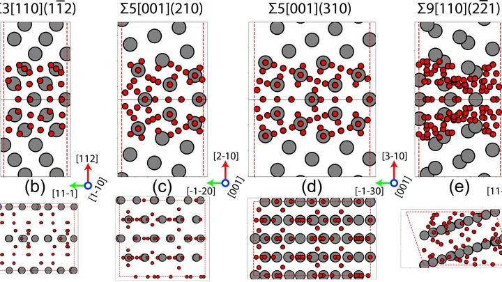
An iron crystal is like a mosaic of tightly packed grains. Where one grain meets another, a boundary forms — a narrow seam with disrupted order. It is in these seams that surprises for magnetism hide.
Scientists calculated how iron atoms interact with each other at three types of such boundaries.
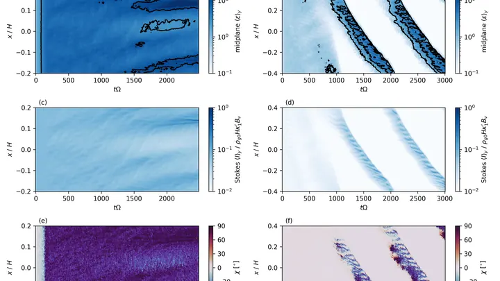
Around young stars, disks of gas and dust swirl — the building blocks for future planets. Inside these disks, dust grains don't just fly randomly: they align along invisible lines of gas flow. Recently, astronomers noticed that dust grains in such disks behave like badminton shuttlecocks — always turning their long side into the wind.
A gold particle a few nanometers across looks like a tiny faceted diamond, but with five faces instead of the usual ones. Inside it hides a defect, like a crack in glass that can either heal or shatter the whole object. Scientists set out to discover what makes this defect move and disappear.
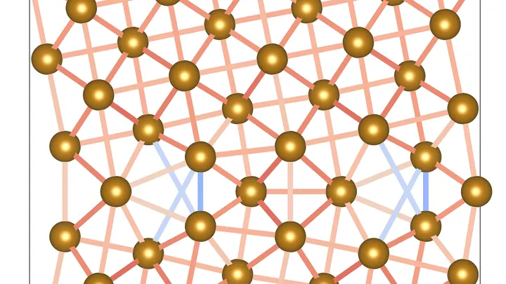
In a thin aluminum film, millions of tiny metal grains are packed together like grains in granite. Where three such grains meet, a triple junction arises — a line along which three boundaries intersect. Previously, it was considered merely a meeting point, but now, peering into the atomic scale, scientists have seen: it is an independent defect with its own personality.