An atomic force microscope (AFM) is a device that images surfaces at the nanoscale by physically 'feeling' them with an extremely sharp tip, rather than using light or electrons. The tip, mounted on a flexible cantilever, is scanned across the sample. As the tip approaches the surface, atomic forces (like van der Waals forces, electrostatic forces, or even chemical bonding) cause the cantilever to bend. By measuring this bending with a laser and photodetector, the AFM builds a topographical map of the surface with atomic resolution. It can work on conductors, insulators, and even living biological samples in liquid.
History
The AFM was invented in 1986 by Gerd Binnig, Calvin Quate, and Christoph Gerber, following Binnig's earlier invention of the scanning tunneling microscope (STM). It quickly became a workhorse in nanoscience because it could image non-conductive samples.
How it works
The AFM operates in several modes. In contact mode, the tip is dragged across the surface and the deflection is kept constant via a feedback loop. In tapping mode, the cantilever oscillates at its resonance frequency and the tip only lightly touches the surface, reducing damage. The key is the feedback system: a computer adjusts the height of the tip to maintain a constant force or amplitude, and the adjustments are recorded as the height profile. This allows the AFM to measure not just topography but also mechanical properties like stiffness and adhesion.
In practice
AFM is used in materials science to characterize thin films, in biology to image DNA and proteins, and in the semiconductor industry to inspect chip surfaces.
Fun fact
The sharpest AFM tips are so fine that they can end in a single atom, allowing researchers to image individual atoms and even manipulate them.
A superconducting quantum interferometer is a device that senses magnetic fields billions of times weaker than the needle of an ordinary compass. Inside it, there is a narrow bridge where superconductivity briefly breaks.
A radio receiver the size of a palm can measure signal power more accurately than expensive lab benches. Inside, there are no coils or antennas, just a glass head and a cloud of rubidium atoms cooled to near absolute zero.
Light flows like an invisible river. If you place an obstacle in the stream, the water whirls into eddies. Likewise, specially designed surfaces create light 'whirlpools' that catch nanoparticles like wood chips.
In a small Petri dish sits a droplet of liquid the size of a pinhead. An ordinary scanner wouldn't even notice it: the signal is too weak. But bring a tiny magnetic field sensor close to the droplet, and the picture changes.
A security guard needs to check five rooms but can't go inside. He knocks on the door and listens: silence means someone is inside, while an echo means the room is empty.
Any cook knows: whether dough sticks to a pan depends on what happens at the interface between two media. For molten metals, that interface long remained invisible — temperatures above 200 °C made it impossible to resolve individual atoms.
Think of a stack of paper: when the sheets lie perfectly aligned, light passes through them uniformly. But turn one sheet by a few degrees, and the picture changes. Something similar happens with layers in certain materials: rotate them relative to each other, and their properties change — sometimes dramatically.
Spectroscopy isn't the key here, or rather, it's not the method used.
The boundary between two liquids is like an invisible skin: it's there, but you can't touch it with your finger. Scientists have found a way to measure its elasticity without touching it. They made a tiny probe oscillate above the surface, and between the probe and the interface lay a thin film of liquid.
A flexible screen as thin as a human hair is glass you can bend. But this marvel has a quirk: touch it, and an invisible electric charge lingers on the surface. Like dust on polished furniture, it builds up and interferes with operation.
A tiny speck of silver is born in a laser beam and immediately starts to grow — faster than you can blink. An ordinary microscope can't keep up with that speed, so until now no one had seen exactly how a nanoparticle appears and gains size. Now scientists have a tool that captures this 'movie' frame by frame.
The tip of a tunneling microscope hovers above a surface at a distance smaller than the diameter of an atom. Usually, it feels out the topography like a finger reading a page of Braille. Now, that same tip has learned to listen to how a membrane the size of a fingernail trembles.
A cell doesn't just lie on a surface: it probes it, pulls it, and pushes it. Until now, instruments could only detect direct forces: how hard a cell presses or stretches its support. But if you grab a cell by the "shoulders" and give it a slight twist, it responds by rotating, and until recently, no one could measure that rotation.
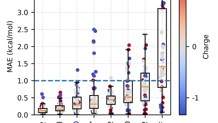
You need to sift through millions of keys to find the one that unlocks the lock of a disease. Each key is a molecule, and the lock is a protein in our body. Checking each key manually is impossible, so chemists use computer models that predict how a molecule will behave in reality. Until recently, accurate calculations took hours or days on powerful computers. The new tool AceFF does it in seconds.