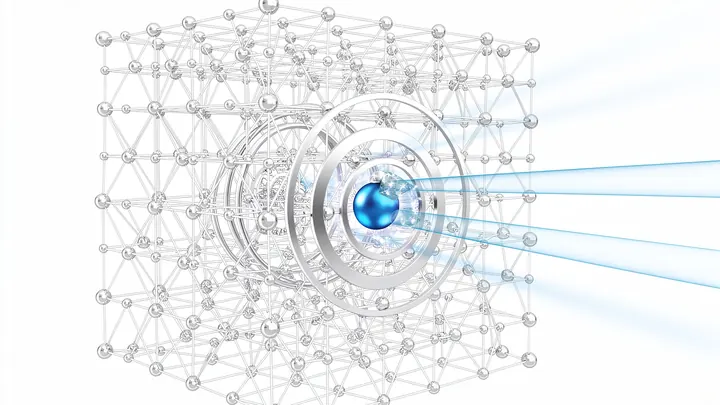
An electron trap is a defect site within a crystal lattice that can capture and hold an electron, preventing it from moving freely. These traps are crucial in semiconductors, where they affect conductivity, and in quantum technologies, where they can serve as stable, addressable quantum bits (qubits). In diamonds, nitrogen-vacancy (NV) centers are a famous example: a nitrogen atom adjacent to a vacancy creates a trap that can hold an electron with a spin state that can be read out optically.
History
The concept of electron traps in crystals emerged in the 1930s–1940s with the development of solid-state physics, particularly through the work on color centers in alkali halides. The NV center in diamond was first characterized in the 1990s and became a major focus for quantum applications in the 2000s.
How it works
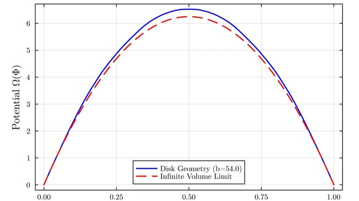
A defect in the crystal structure creates a local potential well—a region of lower energy where an electron can become localized. The electron is held there by electrostatic forces and can be excited to higher energy levels by light or electric fields. The trapped electron's spin state can be manipulated and measured, making it a useful sensor or qubit. The trap's depth and stability depend on the surrounding lattice and the defect's charge state.
In practice
Electron traps are used in quantum computing (as qubits), in high-sensitivity magnetometry and thermometry, and in semiconductor devices to control charge carrier lifetimes. They are also exploited in dosimetry for radiation detection.
Fun fact
The nitrogen-vacancy center in diamond can sense a single electron spin and operates at room temperature, unlike many other quantum systems that require extreme cooling.
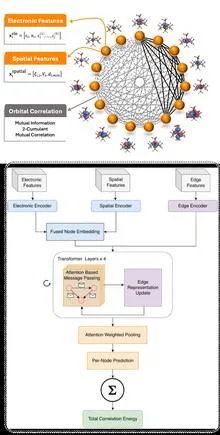
A cartographer who draws not mountains and rivers but invisible bonds between electrons: that's one way to describe the new neural network. Instead of atomic coordinates, it takes molecular orbitals and draws a graph where nodes are orbitals and edges are measures of their quantum entanglement.
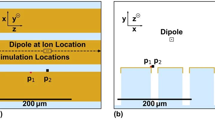
Building a quantum network node is like teaching a dancer to balance on a carbon thread over an abyss. One leg must spring lightly from the wire, hurling photon-messengers into the external world. The other must grip the rope tightly, guarding precious quantum information.
A quantum computer is like an orchestra where each ion is a musician and laser pulses are the conductor's baton. But if someone in the audience rustles, the delicate melody of quantum states goes off key.
In murky mud, between two electrodes, long chains of bacteria line up: each one as thin as a microscopic cable. Every such filament conducts current over a full centimeter, a true marathon for a microbe.
Hundreds of spinning tops sit on a carousel. Each one spins on its own, but the whole carousel also rotates. The challenge is to reach out and tilt the axis of any top as it whizzes by.
In diamond quantum devices, there's a tiny defect — the nitrogen-vacancy center (a nitrogen atom plus a vacancy where a carbon atom should be). It acts as a switch that spontaneously flips back and forth: it can carry an extra electron or not, and this determines whether it emits light or not.
Energy transfer in photosynthesis is like a children's slide: it bends under the weight of one, reshaping the path for the next. That's what happens in a leaf: an excited molecule instantly reshapes the 'landscape' of its neighbors.
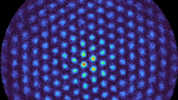
Physicists reproduce this effect using ions suspended in a vacuum trap.
A tiny diamond with a defect — a nitrogen atom next to a vacancy in the crystal lattice. This defect, the NV center, acts like a magnetic needle: under green light, it glows red, and the brightness of that glow depends on the direction of its magnetic field.
A spinning top, set in motion on a perfect surface, topples from the slightest tremor. Likewise, a quantum bit, created at a defect in a diamond, has its state destroyed by magnetic disorder from impurities and external interference.
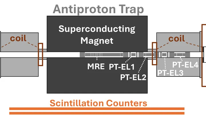
At CERN's antimatter factory, antiprotons are born with the energy of a bullet from a rifle. You can't just put them in a box: they instantly annihilate upon touching ordinary matter. So physicists devised a way to catch them in electromagnetic traps — invisible cages made of fields.
The Sun constantly emits a stream of charged particles — the solar wind. Among them are many electrons, some of which fly back toward the Sun. But observations show that fewer electrons return than expected.
Three charged ytterbium atoms are arranged in a triangle inside an electromagnetic trap. Normally, they all communicate with each other, like three people at a table constantly exchanging remarks. But if one of them steps into the next room, the conversation continues between the remaining two.
A diamond speck smaller than a hundredth of a millimeter glows red. Inside it is a crystal defect: two neighboring carbon atoms, where one is missing and a nitrogen atom sits nearby. Such a pair captures light and re-emits it, like a tiny beacon that doesn't fade at room temperature.
This speck was brought near a pathway on the chip's surface.
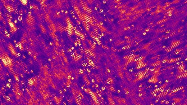
In NaAlSi, as it cools, electrons form fleeting ripples — stripes that appear and vanish, like patterns on water stirred by wind. These stripes intertwine with superconductivity, a state where current flows without resistance. Typically, for this, electrons pair up with uniform binding energy.
Metals are full of free electrons: they dart between atoms like a swarm of bees around a hive. If you poke such a metal with a thin magnetic filament, the electrons start to feel its field. A new calculation shows they don't just go around the field; they trap it inside, like a cork sealing water in a bottle.
A tiny diamond, smaller than a dust speck, hovers inside a magnetic trap made of microchips. Inside the crystal is a single defect acting as a beacon. Scientists coax the diamond into being in two places at once, like a magician’s ball that honestly rests under two cups.
This isn't just a trick.
Every breath you take and every muscle twitch runs on a stream of electrons flowing through proteins inside your cells. These proteins aren't static: they constantly change shape, like a spring that compresses and releases. But until now, no one has seen exactly how these movements open or close the path for electrons.
Quantum computers demand reliable memory. In a diamond crystal — carbon — information is stored as the orientation of microscopic magnetic needles (spins) at special defects. Reading these arrows with light was inconvenient: optics are bulky for chips. The new method works like developing photographic film.
Inside a diamond, you sometimes find tiny flaws — a spot where a carbon atom is replaced by nitrogen, with a vacancy right next to it. Physicists call this an NV center (a nitrogen-vacancy defect). Such a defect acts like a magnetic needle that can store information in its spin.
A tuning fork sounds when you strike it. Its prongs vibrate, and you hear the sound until the vibration dies out. The quantum world has its own "tuning forks"—for example, a defect in diamond that responds to magnetic fields, and a carbon tube that can tremble at frequencies billions of times higher than the note A.
Hidden within the bulk of a diamond are tiny flaws — places where a carbon atom is replaced by nitrogen, with a vacancy gaping nearby. These defects, like beacons, can store and transmit quantum information. But around them rages a magnetic storm: the nuclei of atoms in the crystal jostle, creating interference.
A superconducting qubit, a tiny loop with zero resistance, crunches problems faster than you can blink. But cut the power, and everything it has calculated vanishes. Like a chef who cooks without writing down the recipe: as long as he's at the stove, he remembers every step, but an hour later — nothing.
The authors of the study propose writing the result into diamond.